Vision Types Split First by Wavelength and Pixel Size
OPTICS
A 50 μm defect spans a little over two pixels in a visible-light camera and only 0.32 of a pixel in a thermal camera.
Put one board under six types of vision and the calculation shows that what separates them is what each one reads and how large one pixel is, rather than the camera’s name.
About 16 min read
Suppose a 100 mm square board sits on the inspection stage. Its surface is covered with green solder mask that scatters light evenly in all directions, close to matte, and I assume its reflectance1 is middling. Only the copper pads show up here and there as smooth, specular patches. Four things have to be found on this board: a scratch 50 μm wide, a solder joint with a 20 μm height deviation, a crack inside a chip, and a part that runs unusually hot once power is applied. The list and the sizes are assumptions I set for the calculation.
Hand all four to one camera and one of them is bound to slip through. A scratch shows up as a difference in the intensity of reflected light, a height deviation as a difference in distance, a crack inside a chip as a difference in how much light passes through, and overheating as a difference in the light a part emits by itself. A missed scratch ships in the good bin, and a missed hot part comes back as a failure inside a customer’s device. So choosing vision starts with deciding what to read, before choosing a camera model. The vision types part ways along that answer.
The six vision types are visible-light area scan, line scan, 3D profile, stereo depth, SWIR and LWIR thermal. In the same 100 mm field of view I calculate the size of one pixel, the height resolution and the diffraction limit, and set them side by side. One question remains at the end: how many of the six can see a 50 μm defect?
Six types of vision read one of four physical quantities
What a camera turns into a picture is, in the end, the amount and position of light reaching the sensor. Where that light came from divides the vision types. Visible-light area scan and line scan read the intensity of the lamp’s light bounced off the surface, and SWIR cameras also read reflected light, which puts them in the same family. The RP Photonics buyer’s guide separates NIR and SWIR cameras, which mostly image reflected light, from MWIR and LWIR cameras, which see heat radiation.
3D methods read position instead of intensity. Laser triangulation2 turns how far an obliquely viewed laser line bends into height, and stereo3 turns how far the same point shifts between two pictures into height. Reflectance, distance, transmittance and emission: which of these four carries the trace of the defect is the first fork, and size comes after.
Visible-light area scan competes on the size of one pixel
Area scan4 is the most familiar type, one shot for one picture. Assume a 100 mm field of view and 4,096 px across the sensor, and one pixel covers 100 mm ÷ 4,096 = 24.41 μm. A 50 μm scratch therefore spans 2.05 pixels. A pixel pitch of 3.45 μm and a 25 mm lens are also assumptions; together they give a sensor width of 14.13 mm and a magnification of 0.141. The WD5 is 25 mm × (1 + 1 ÷ 0.141) = 201.9 mm.
Calling a defect seen when it spans two pixels is the loosest standard, and I trust the number only when a feature fills three. On a three-pixel basis the smallest identifiable size of this setup is 73.2 μm, so the 50 μm scratch shows up only conditionally. Lighting is part of that condition. If I assume the reflectance difference of a scratch on solder mask is small, a dome light that illuminates the whole surface evenly has the advantage, but whether to add coaxial lighting where specular reflection from copper pads blows out to white is something to confirm with sample images.
Halve the field of view and one pixel becomes 12.2 μm, bringing the three-pixel size down to 36.6 μm. In exchange one board has to be shot in four tiles, so inspection time quadruples. Line scan takes another road.
Line scan turns motion into pixels
Line scan6 uses a sensor with a single row of pixels and stacks lines while the sample passes by. With an 8,192 px sensor (5 μm pixels, 40.96 mm long) and a 50 mm lens, the magnification is 0.41, the WD is 172.1 mm, and in a 100 mm field one pixel is 12.21 μm. A 50 μm scratch spans 4.1 pixels, and the smallest identifiable size on a three-pixel basis is 36.6 μm. By this calculation one pixel is half the size of area scan in the same field, because one sensor gathers 8,192 pixels across at once.
To make one pixel square on a moving sample, the line readout speed has to match the sample speed. Assume the sample passes at 0.5 m/s and the line rate is 0.5 m/s ÷ 12.21 μm = 40.96 kHz, with at most 24.41 μs of exposure per line. The Vision Systems article on line scan cameras works the same arithmetic. A 40 MHz clock with a 2,048 px sensor gives 19.5 kHz, and at 1 m/s one pixel along the direction of travel becomes 51.28 μm, so the pixel is flattened.
12.21μm
One pixel in line scan (100 mm field, 8,192 px)
40.96kHz
Line rate needed at 0.5 m/s (assumed)
204.8×
Light needed versus a 5 ms area scan exposure (assumed)
The third number is the price of line scan. With exposure cut to 24.41 μs, the light area scan used at 5 ms (assumed) has to be fired 204.8 times harder to reach the same brightness. Line scan has the advantage when the sample passes at a steady speed in one direction, an encoder signal reports position along the travel, and there is room for a strong line light. If one of the three is missing, the gain disappears.
3D reads height, but the orders of magnitude differ
A 20 μm height deviation in solder is hard to pick out from picture brightness. That is where 3D methods that read position come in, and even among 3D vision types, laser triangulation and stereo differ in height resolution by a factor of 26 under these assumptions. I calculate the laser first. With a 100 mm field, a 4,096 px sensor (5 μm pixels) and a 25 mm lens, the WD is 147.1 mm and one pixel across is 24.41 μm.
Fire the laser vertically onto the board and tilt the camera by 30°, and a height change of h appears to the camera as a shift of h × sin 30°. One pixel therefore stands for 24.41 μm ÷ 0.5 = 48.83 μm of height. Locating the center of the laser line to a fraction of a pixel (sub-pixel, assumed at 1/10 pixel) gives 4.88 μm, so a 20 μm deviation is read with about 4.1 times to spare. This is an idealized assumption and it shrinks if specular reflection from copper pads or solder gloss smears the laser line. Because the surface is glossy, it cannot be guaranteed before a sample test.
Give the same 20 μm to stereo. Height error grows as ΔZ = Z² × Δd ÷ (f × B). A baseline B of 50 mm, a focal length of 1,400 px and a disparity error Δd of 0.1 px are assumptions, and at Z = 300 mm the error is 128.6 μm, at 600 mm it is 514.3 μm. That is 6.4 times coarser than the 20 μm target. Double the distance and the error quadruples, so stereo suits guiding position in millimeters and does not suit measuring height in micrometers.
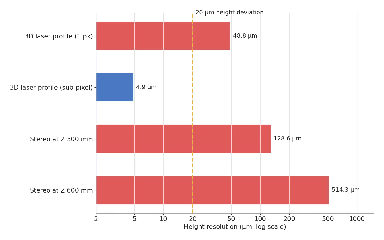
What I look at first in the figure is the left and right sides of the yellow dashed line. Only one bar lands left of the 20 μm line, the laser with sub-pixel processing, and the same laser read at one whole pixel slips to the right of it. Both stereo bars sit far to the right. ToF (which times the light’s return) is listed by Photoneo with errors from millimeters up to centimeters, which puts it further right, off this graph. VA Imaging says structured light is precise but sensitive to ambient light and reflective surfaces, and Photoneo says methods that take several frames need the sample to stay still.
The three have separate places to work. Stereo and ToF suit a robot picking up large textured objects, laser suits the height profile of a moving sample, and structured light suits precise measurement of small parts that sit still. The moment solder height is set at 20 μm I would drop stereo and put laser and structured light head to head on samples.
Invisible wavelengths hit the wall at the wavelength first
Now the crack inside a chip and the hot part. Silicon sensors stop responding near 1 μm, so longer wavelengths belong to SWIR7 cameras with InGaAs sensors. The inspectandtest guide to SWIR says silicon becomes partly transparent in this band (roughly 0.9 to 1.7 μm), which helps electronics inspection. Whether a crack inside a chip actually shows depends on the chip’s structure and is something to confirm on samples. The same guide notes that SWIR reads reflected light and so needs a dedicated lamp, and that prices run from thousands to tens of thousands of dollars depending on resolution.
The hot part belongs to the LWIR8 thermal camera. In the 8 to 14 μm band a microbolometer sensor reads the heat radiation the part emits by itself, and the ability to separate temperatures is expressed as NETD9. RP Photonics gives less than 30 mK as an example of a low value. A thermal camera reads temperature more than shape, though. Shiny metal has low emissivity10 and shows colder than it is, a point worked out separately in the article on shiny parts and thermal cameras.
Neither solves the problem of size. Put a 640×512 px sensor on the same 100 mm field and one pixel is 100 mm ÷ 640 = 156.25 μm, which makes a 50 μm defect 0.32 of a pixel. To see 50 μm across two pixels the field has to shrink to 640 × 25 μm = 16.0 mm. Pixel pitches of 15 μm (SWIR) and 12 μm (LWIR) and a 25 mm lens are assumptions, and the WD then comes to 285.4 mm for SWIR and 350.5 mm for LWIR.
One could ask whether a sensor with smaller pixels would do, but the lens comes first. A lens blurs a point into an Airy disk11 whose diameter is about 2.44 × wavelength × f-number. With every f-number set to 2, visible light (0.55 μm) gives 2.68 μm, SWIR (1.55 μm) gives 7.56 μm and LWIR (10 μm) gives 48.8 μm.
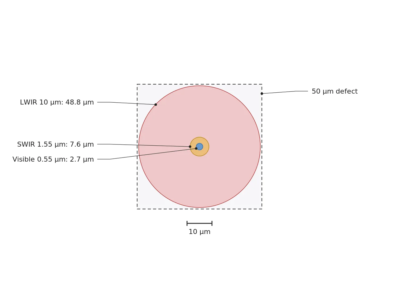
What I look at first in the figure is where the red circle nearly fills the dashed square. The LWIR blur of 48.8 μm is 0.98 times the defect size, so however small the pixels are made, one blurred spot of light grows to the size of one defect and the outline is erased. The blue circle (visible light) is 5.4 % of the defect at the same spot. This limit is set by wavelength, so it is not lifted by raising the lens grade or the pixel count.
Belief
A higher-resolution camera lets you see smaller defects.
Reality
Against a 50 μm defect, LWIR blurs to 48.8 μm at f/2, so wavelength sets the limit before pixel count does.
Putting the six types on one table
Set against the same field and the same defect, each type’s place shows. The figure below lines up twice the pixel size, the smallest length each type can tell apart, on one scale.
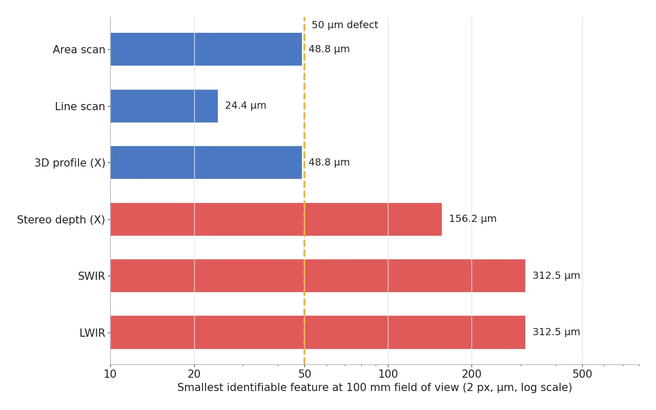
What catches the eye first in the figure is the three red bars right of the yellow dashed line. Stereo at 156 μm and SWIR and LWIR at 312.5 μm cannot hold a 50 μm defect inside one pixel. Left of the line, area scan at 48.8 μm and the lateral value of the 3D profile at 48.8 μm sit on the theoretical limit, and only line scan at 24.4 μm has room to spare. Bundled into one specification table, the numbers read as follows.
| Vision type | ① Smallest identifiable size | ② Optical setup · WD | ③ Algorithm parameters · In plain words |
|---|---|---|---|
| Visible-light area scan | 48.8 μm (2 px), 73.2 μm (3 px). 24.41 μm/px | Dome or coaxial lighting, 25 mm lens, WD 201.9 mm (confirm in the data sheet) | Minimum blob area 4 px, brightness-difference threshold set on samples. A 50 μm scratch is just over two pixels, so it is borderline |
| Line scan | 24.4 μm (2 px), 36.6 μm (3 px). 12.21 μm/px | Line light, 50 mm lens, WD 172.1 mm | Encoder division so 1 line = 12.21 μm, line rate 40.96 kHz, exposure at most 24.41 μs. A 50 μm defect is four pixels, so there is room |
| 3D profile (laser) | Lateral 48.8 μm, height 4.88 μm (sub-pixel 1/10 px assumed) | Laser line, 25 mm lens, WD 147.1 mm, triangulation angle 30° | Peak detection at 1/10 px, height decision width ±20 μm. A 20 μm step is read with 4 times to spare |
| Stereo depth | Height 128.6 μm (Z 300 mm), lateral 156 μm | Baseline 50 mm, focal length 1,400 px, texture to be confirmed | Disparity error 0.1 px (assumed). A 20 μm step is 6.4 times too coarse, so it does not fit |
| SWIR | 312.5 μm (2 px). 50 μm = 2 px at a 16.0 mm field | 0.9 to 1.7 μm InGaAs, SWIR lamp, 25 mm lens, WD 285.4 mm | Filter band and contrast threshold set on samples. It may see into a chip, but a 50 μm scratch needs a smaller field |
| LWIR thermal | 312.5 μm (2 px). Diffraction limit 48.8 μm (f/2) | 8 to 14 μm microbolometer, 25 mm lens, WD 350.5 mm | Emissivity correction, alarm width ΔT (confirm the NETD spec). An eye that reads temperature more than shape |
What the six rows say is that each vision type is compared on a different yardstick. Area and line scan compete on size, 3D on height, and the two infrared types on transmission and temperature, so squeezing them into one ranking gets it wrong. There are conditions where the opposite approach wins. If the defect is over 2 mm and pixel size is not an issue, one cheap area scan camera is better, and if the height tolerance is 1 mm or more, stereo is reasonable. This judgment cannot be guaranteed before a sample test, and once the assumed values in the table are replaced with the field and sensor of a real station, each row has to be recalculated.
The order of choosing and who pays
The order of choosing is short. First decide whether the defect shows in reflectance, height, transmission or temperature, then calculate the size of one pixel, and last confirm the WD and the lighting. To anyone starting out in this work I recommend doing by hand, before memorizing the names of vision types, the one-line calculation of dividing the field by the pixel count. The same board with the shutter, the color and the cable changed is worked out in the article comparing camera types.
The job that makes this choice is the machine vision engineer, and because each vision type reads differently, a person who can tell the four physical quantities apart talks more easily on site than one who knows a single type. Cost has a different structure for each vision type. Line scan brings a strong line light and an encoder, infrared brings dedicated optics and lighting, and SWIR is costly in the sensor itself, as the guide’s thousands to tens of thousands of dollars suggests. This article explains technology and is not investment advice. See our Disclaimer.
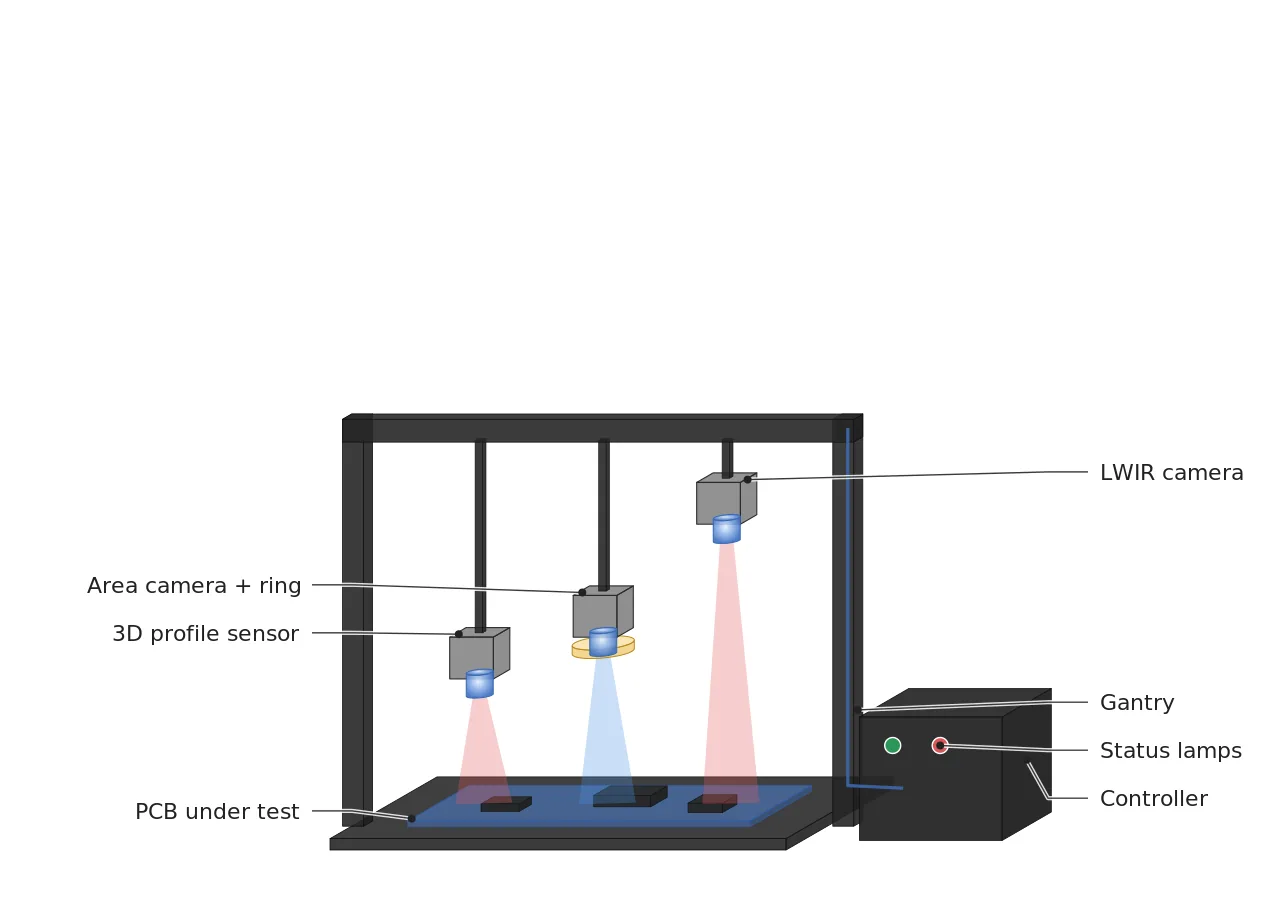
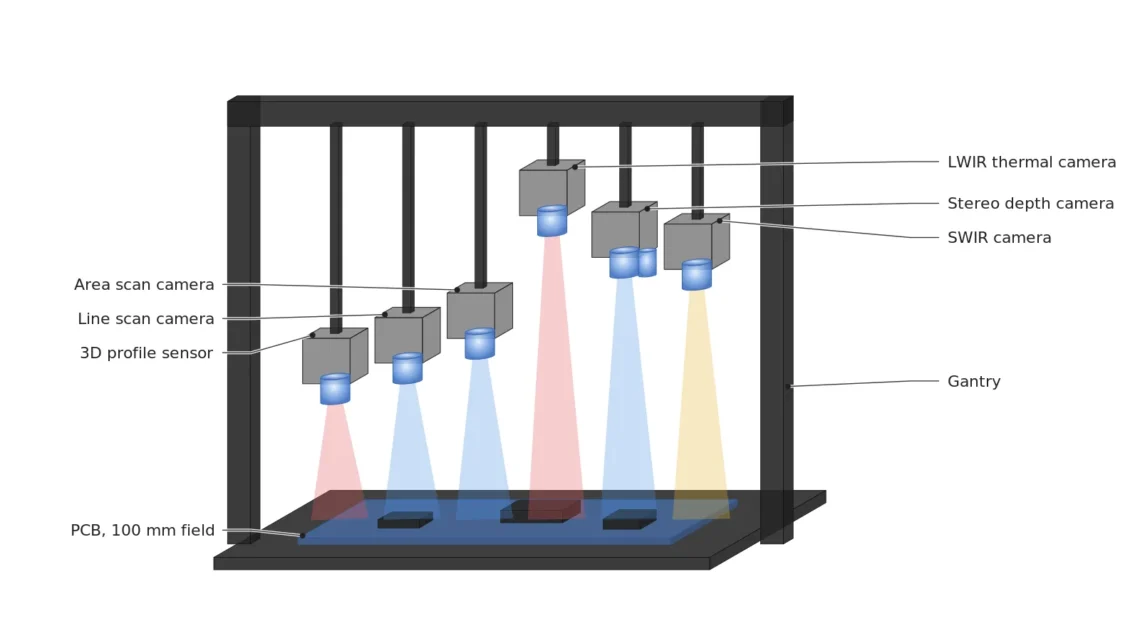
The figure shows an inspection station with three types stacked over one fixture. Lens height varies with the WD, so between the lowest laser (147.1 mm) and the highest thermal camera (350.5 mm) there is a gap of over 20 cm, and whether one gantry can hold that height difference is the first question to settle early in design.
Field Note
What the viewfinder of a film camera shows is not quite what lands on the film, so I frame through the viewfinder and still check the developed result. Inspection is the same: choose a vision type from the numbers in the data sheet, then check again with sample images. My start on a new board is one visible-light area scan camera. I read the spread of appearance defects first, and I add a laser or thermal camera one at a time, and only when the missed defects cluster in height or temperature. Mount all six at the start and I cannot tell which one caught what.
Field Checkpoints
After choosing a type, what remains is striking off installation conditions one by one.
- Is the WD from lens to board top (area 201.9 mm, line 172.1 mm, laser 147.1 mm, SWIR 285.4 mm, LWIR 350.5 mm) still secured after adding the fixture and the lighting? (does room remain for lamps and hands)
- Is the size of the defect to be found at least three pixels (my standard)? (is this the border where the field has to shrink or line scan has to take over)
- Is the height tolerance fixed, and does the height resolution of the chosen 3D type fall within a quarter of it? (for stereo, does the tolerance accept 128.6 μm at a distance of 300 mm)
- Have specular spots such as copper pads and solder been checked on sample images? (are glossy surfaces left unconfirmed by calculation alone)
- For line scan, are an encoder signal and a line light that gives exposure of 24.41 μs or less secured? (is the lamp replacement interval in the plan)
- For infrared, can the field be cut to around 16.0 mm? (if not, is the 50 μm defect dropped from the detection targets)
Glossary
- [1] Reflectance reflectance
The share of the light reaching a surface that comes back off it. White paper is high and black cloth is low. ↩ - [2] Laser triangulation laser triangulation
A method that projects a thin laser line and reads height from how far the line, seen at an angle, appears bent. The sample or sensor moves and the profile is collected line by line. ↩ - [3] Stereo stereo vision
Distance is calculated from how far the same point shifts between two pictures taken by two cameras (disparity), as with human eyes. ↩ - [4] Area scan area scan camera
A camera whose sensor has pixels laid out in rows and columns and takes one whole picture per shot, like a smartphone camera. ↩ - [5] WD working distance
The distance from the lens to the top of the part being inspected. The text calculates it with a thin-lens approximation from the principal plane, and the reference plane a maker uses has to be checked in the data sheet. ↩ - [6] Line scan line scan camera
A camera with a single row of pixels that builds a picture by stacking lines while the sample passes by. ↩ - [7] SWIR short-wave infrared
Infrared light with a wavelength of roughly 0.9 to 1.7 μm. It images reflected light like an ordinary camera, and the sensor is usually InGaAs. ↩ - [8] LWIR long-wave infrared
Infrared light of roughly 8 to 14 μm, where the camera reads the heat radiation an object gives off by itself. ↩ - [9] NETD noise equivalent temperature difference
The smallest temperature difference a thermal camera can tell apart. The smaller the number, the finer the difference it sees. ↩ - [10] Emissivity emissivity
The fraction of heat an object radiates compared with an ideal radiator at the same temperature, from 0 to 1. Shiny metal is low and looks colder than it is. ↩ - [11] Airy disk Airy disk
The small disk into which a lens blurs a point of light. Its diameter is about 2.44 × wavelength × f-number. ↩
References
- RP Photonics, Buyer’s Guide: Infrared Cameras (sensor types by band, resolutions, NETD example, optical materials), accessed October 14, 2026
- inspectandtest.net, Short-wave infrared camera (SWIR band, InGaAs sensors, silicon transparency, price range), accessed October 14, 2026
- Vision Systems, Choosing a line scan camera for web inspection applications (line rate and resolution worked example, lighting needs), accessed October 14, 2026
- VA Imaging, Which 3D Camera Technologies Do I Need? (strengths and weaknesses of stereo, structured light, ToF and laser triangulation), accessed October 14, 2026
- Photoneo, Major 3D sensing technologies (ToF error range, static-scene condition for multi-frame structured light, manufacturer material), accessed October 14, 2026
- Formulas: pixel footprint = field ÷ horizontal pixel count, magnification = sensor width ÷ field, WD = f × (1 + 1 ÷ magnification), line rate = sample speed ÷ pixel footprint, laser triangulation height resolution = pixel footprint ÷ sin(triangulation angle), stereo height error ΔZ = Z² × Δd ÷ (f × B), Airy disk diameter = 2.44 × wavelength × f-number

Noctvision
An engineer who designs secondary-battery manufacturing equipment keeps this record while studying local AI on single-board computers such as the Raspberry Pi and Jetson.


You May Also Like
Adding Cameras to a Semiconductor/PCB Inspection Line: The Interface Rewrites the Optical Design
Catching 20 μm Sink Marks in High-Gloss Injection-Molded Parts with Phase Measuring Deflectometry (PMD) — The Last Gap Polarization Fusion Fills