In SWIR, One Stop Down Erases a 3.4 μm Pixel
OPTICS
At 1800 nm, a fully open f/2.8 leaves only 15 % contrast on a 3.4 μm pixel, and one stop down takes it to zero.
The habit of stopping down a SWIR lens to buy depth of field gets more expensive as the wavelength grows. Write down wavelength, pixel size and part height spread first.
About 14 min read
The idea that closing the aperture by one stop makes the picture sharper has served well for a long time in visible light, because the range in front of and behind the focus widens. Carry that habit straight over to a short-wave infrared (SWIR)1 camera and the result goes the other way. On October 5, Schneider-Kreuznach introduced CHROMITE, a 12 mm f/2.8 C-mount SWIR lens that covers 400 to 1800 nm without refocusing, and said it supports sensors with pixels down to 3.4 μm. Now that one lens can move between visible light and SWIR so easily, it is also time to work out why the same aperture value gives such different results at different wavelengths.
The inspection target is the copper pads and solder resist on a PCB, and a black molded connector housing. A smooth copper pad tends to show strong specular reflection2, which sends light back in a single direction, so whether a 160 μm3 foreign particle on it shows up in SWIR cannot be guaranteed before a sample test. A reflectance figure cannot be written down while it is unconfirmed, so what follows calculates only the limit set by the lens and the pixel, whatever the material. Stop down without knowing that limit and you gain depth of field but the particle on the copper pad smears away, and a bad board slips into the pass box.
Before touching the aperture, I would write down three numbers: the wavelength of the light, the pixel size of the sensor, and the spread of part heights inside the field of view. With those three on paper, a few taps on a calculator show how far a given lens can keep the pixels alive.
Even a perfect lens cannot turn a point into a point
Water waves passing through a gap in a breakwater fan out behind it, and the narrower the gap, the wider they spread. Light does the same, so a point source passing through a round aperture lands not as a point but as a disk, the Airy disk4. The diameter of the disk is 2.44 × wavelength × F-number5. Even when the lens design has removed every chromatic and spherical aberration, this spreading stays, so the limit is called the diffraction limit6. The longer the wavelength, the bigger the disk.
With a 3.4 μm pixel sensor and f/2.8 held open, the disk is 3.76 μm at 550 nm, about 1.1 pixels. At the same f/2.8 it grows to 6.4 μm or 1.9 pixels at 940 nm, 10.6 μm or 3.1 pixels at 1550 nm, and 12.3 μm or 3.6 pixels at 1800 nm. A single point covers three and a half pixels, so the light is read mixed across several neighbouring pixels. This calculation assumes an ideal lens with no aberrations, so a real lens cannot exceed it.
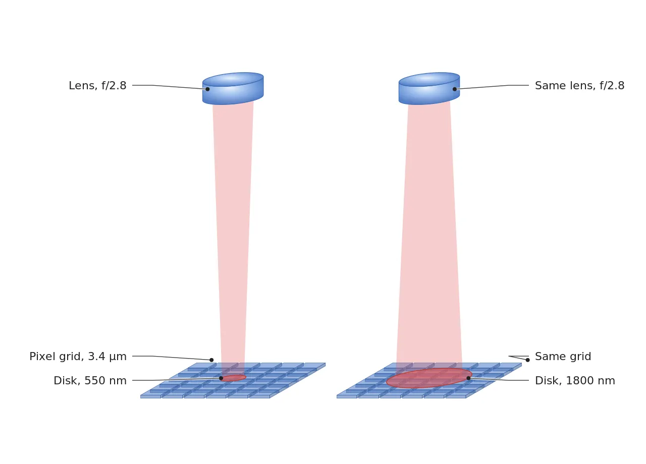
What I look at first in the figure is the difference in size between the two disks. The left disk is a little over one pixel, so little light spills into neighbours, while the right disk covers three and a half cells of the grid and blends into them as one lump. Same lens, same aperture; the only thing that changed is the wavelength.
12.3μm
Airy disk diameter at 1800 nm, f/2.8
3.6px
Number of 3.4 μm pixels that disk covers
3.76μm
Diameter at the same f/2.8, 550 nm
How much of the pixel stripes survive is set by wavelength
The finest stripes a pixel can tell apart are one bright pixel followed by one dark pixel, and the density of that pattern is the Nyquist frequency7. For a 3.4 μm pixel it is 1 ÷ (2 × 0.0034 mm), or 147 lp/mm. A striped shirt seen from far away melts into one grey sheet, and in the same way, if the lens smears these stripes, a sensor with any number of pixels receives only a grey with no contrast. The percentage of contrast that survives after the lens is the MTF8.
The MTF of a diffraction-limited lens comes out in closed form. Put the cutoff frequency ν_c = 1 ÷ (wavelength × F-number) and x = 147 ÷ ν_c, and MTF = (2÷π) × (arccos x − x × √(1−x²)), which is 0 once x passes 1. Put f/2.8 into this and the contrast left at Nyquist is 71 % at 550 nm, 52 % at 940 nm, 35 % at 1310 nm, 25 % at 1550 nm and 15 % at 1800 nm. The F-number at which the stripes are erased outright is 2 × pixel ÷ wavelength: f/12.4 at 550 nm, f/7.2 at 940 nm, f/4.4 at 1550 nm and f/3.8 at 1800 nm.
These values are an upper bound that counts only the lens diffraction. Losses at the sensor pixel aperture and lens aberrations cut further, so I read real contrast as lower than these numbers. My own floor is 30 % contrast at Nyquist. The F-numbers that hold that line are f/7.2 at 550 nm, f/4.2 at 940 nm, f/3.0 at 1310 nm, f/2.6 at 1550 nm and f/2.2 at 1800 nm. The f/2.2 at 1800 nm is a value this lens, whose widest aperture is f/2.8, cannot reach, so a 3.4 μm pixel at 1800 nm starts below the 30 % line even with the lens wide open. The product of wavelength and F-number on the 30 % line stays near 3.98 μm, so the longest wavelength at which this lens held open can keep 30 % is 3.98 ÷ 2.8, about 1420 nm.
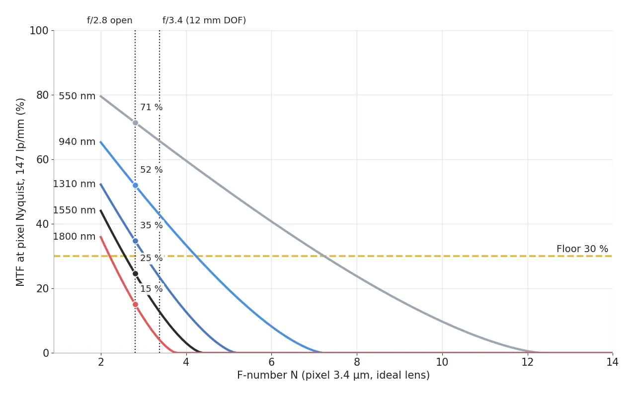
In the graph, the wavelength curves lean further left as they get longer, and the F-number at which each meets the yellow 30 % line differs by wavelength. The curve on the visible side meets the yellow line only near f/7, while the 1800 nm curve already meets it at f/2.2 and sits far below it to the right of f/2.8, the open position of the lens. The scale reads the same F-number, yet the value read off it changes this much with wavelength.
Where one stop is enough to erase the stripes
The aperture blades of a film camera are several thin metal plates that overlap to form the opening, and each time the opening diameter shrinks by a factor of √2 it is said to be stopped down by one stop. Going from f/2.8 to f/4 is one stop, and the light that gets in falls to 1/2.04. In visible light the price of that one stop is small, as 550 nm contrast drops only from 71 % to 59 %, 12 percentage points.
The same one stop turns 25 % into 3 % at 1550 nm and 15 % into 0 at 1800 nm. At 940 nm it goes from 52 % to 33 %, and at 1310 nm from 35 % to 13 %, so even the NIR side that sat above the 30 % line falls below it the moment you stop down one stop. A SWIR lens stopped down one stop gives a frame with half the brightness and, at 1550 nm and beyond, stripes erased as well, so I read that one stop less as a price paid for depth and more as handing contrast over wholesale. A component whose contrast has reached 0 cannot be revived by any filter, and pulling up one with only 4 % left raises the noise by the same ratio.
Putting a 12 mm height spread and 15 % contrast on one scale
So where does the depth come from? Depth of field9 is 2 × F-number × circle of confusion10 × (m+1) ÷ m², where m is the magnification. Take 6.8 μm, two pixels, as the circle of confusion, and use the 12 mm lens at a WD11 of 200 mm: m is 0.064 and one pixel on the object side is 53 μm. At f/2.8 the depth of field is 9.9 mm, at f/4 it is 14.2 mm, and at f/5.6 it is 19.9 mm. The 200 mm is the closest working distance the maker states for this lens, so note too that there is no room to spare for stand sag or board warp. That makes this spot tight.
If the part heights in the field spread over 12 mm, the F-number needed is f/3.4. The light drops by 1.46 times, and the contrast at Nyquist holds at 66 % at 550 nm and 43 % at 940 nm, but falls to 23 % at 1310 nm, 13 % at 1550 nm and 4 % at 1800 nm, below the 30 % line. Keeping 12 mm of depth and 30 % contrast together works only up to 940 nm. I treat that line as the first constraint of the design.
Since the product of F-number and wavelength is constant, one more line follows. Depth of field is proportional to the F-number, so the depth that holds 30 % contrast is inversely proportional to wavelength, at 25.7 mm at 550 nm, 15.0 mm at 940 nm, 10.8 mm at 1310 nm, 9.1 mm at 1550 nm and 7.8 mm at 1800 nm. The longest wavelength that can cover 12 mm is about 1180 nm, and that line hardly moves when the pixel size changes. Build the same 53 μm object-side pixel with a 5 μm sensor (WD 140 mm) and the depth at 1800 nm is 8.1 mm, so switching to a larger pixel alone does not lift this ceiling.
What is left to turn once the aperture is out
Once the aperture of a SWIR lens is blocked, three knobs are left. The first is choosing a shorter wavelength. The strength of this lens is that you can change wavelength without refocusing, which makes it easy to shoot the same board at 940 nm and 1310 nm and compare which shows the particle more clearly. Copper and solder resist look different at each wavelength, so which one wins is something to decide after shooting samples.
The second is shrinking the height spread itself. Press the board onto a vacuum plate or clamps to take out warp, split tall connectors into separate zones, and if each zone keeps its height spread within 9 mm, focus covers the whole zone even with f/2.8 held open. The third is splitting the height range in two and shooting twice. More shots make each board take longer, so exposure time and judgment time have to be weighed together when you use it.
Leaning on software correction is closed off here. Stripes whose contrast has been pushed toward 0 by diffraction bring their noise up with them when a filter lifts them, and at 0 the information itself is gone. An algorithm cannot get past the limit that the optical setup sets, so the judgment parameters have to be chosen inside the optical limit. That is as far as my judgment goes.
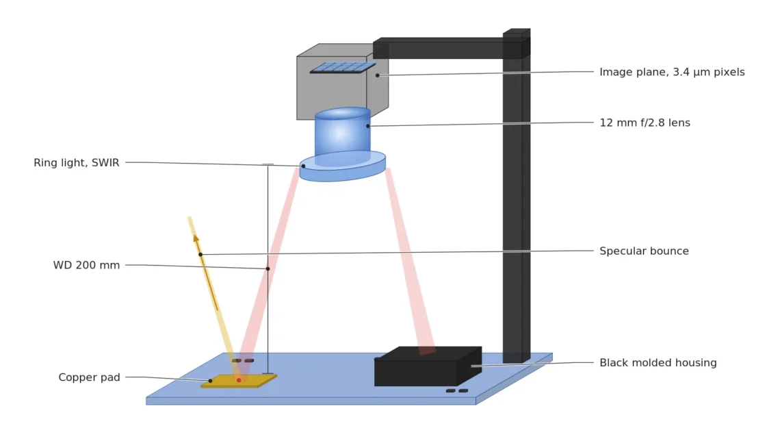
A setup with the lens hung 200 mm above the board
Carry the calculation over to the inspection station and the lens is fixed 200 mm above the board, with the board pressed onto a vacuum plate so that the height spread is within 9 mm. The smallest particle, the optical conditions and the judgment rule are written one line each in the table below.
| Item | Value | Condition and basis | In plain words |
|---|---|---|---|
| ① Minimum defect size | Foreign particle or scratch width on a copper pad: 160 μm | Object-side pixel 53 μm × 3 pixels (Noctvision criterion, pixel 3.4 μm, magnification 0.064 assumed) | A particle has to be three pixels wide to be read |
| ② Optical setup | 12 mm f/2.8 C-mount SWIR lens, pixel 3.4 μm, 1310 nm diffuse illumination, WD 200 mm (the minimum in the lens specification, so no room for sag; confirm the mounting height on a sample), height spread 9 mm or less | f/2.8 wide open, Nyquist contrast 35 % (diffraction-limit upper bound), depth of field 9.9 mm (circle of confusion 6.8 μm), specular reflection of copper cannot be guaranteed before a sample test | Keep the aperture open and solve it by matching the height |
| ③ Algorithm parameters | Region at or below pad mean − 3σ after flat-field correction, minimum connected area 3 px², exposure with f/2.8 fixed, hold the judgment if the sharpness (edge contrast) of a region falls below the criterion | Judge particles only at 30 % contrast or higher, re-shoot or hold below that (Noctvision criterion, tune parameters on samples) | A cell without enough sharpness is not counted as a pass |
Because the end of the wavelengths that can hold the 30 % line with f/2.8 open is about 1420 nm, the illumination is set at 1310 nm with some margin. Still, 35 % is only 5 percentage points above the 30 % line, and losses at the sensor and in aberrations cut that value further, so the hold rule can start working on the first day. To say this setup separates a 160 μm particle, you need numbers from measuring edge contrast on real samples.
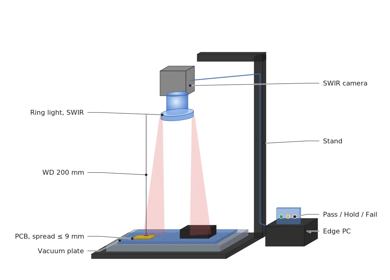
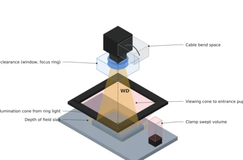
In the figure the lens height is set to a WD of 200 mm, and the board lies flat, pressed onto the vacuum plate. If the particle criterion drops below 100 μm, or the height spread cannot be brought inside 9 mm, a configuration that adds a separate visible-light camera or a 3D profiler that reads height on its own may be more favourable than a SWIR-only setup. Which is right can be said only after shooting samples.
Who does the calculation and who pays for it
Deciding where to put the aperture of a SWIR lens and where to set the wavelength falls to the machine vision engineer in charge of the optical setup. It covers choosing the lens and the illumination wavelength through to measuring edge contrast and setting the judgment criterion. If you are learning this job, I would have you get the one-line Airy disk diameter, 2.44 × wavelength × F-number, and the formula for Nyquist contrast into your hands first. The lens name may change, but those two keep working.
Seen from the side that pays for the equipment, this calculation puts new lines on the quotation. The wavelength and output specification of dedicated SWIR illumination, a vacuum jig that holds the board height within 9 mm, and a first sample test that measures edge contrast per wavelength all become line items. A design that covers visible light through SWIR with one lens has to correct chromatic aberration across the whole band, and has been the subject of patents such as US 10,620,408 B2, which deals with 450 to 2450 nm, but diffraction is a value set outside that design. This article explains technology and is not investment advice. See our Disclaimer.
Field Note
When a new board arrives, I stand a comb-pattern chart at each end of the height range and shoot first at f/2.8 and 1310 nm. The calculated 35 % is an upper bound, so if both charts land between 25 and 35 % I read that as normal, and if one is below half of that I suspect focus position or height spread. Until I have seen those two numbers I do not enter a particle judgment value.
Field Checkpoints
If the two numbers from the charts stay near the calculation, the next step is to fix the lens position. Check these five before tightening the stand that carries the lens.
- Is the WD between the lens reference plane and the top of the copper pad secured at 200 mm or more, and does it stay above that value even after adding stand sag and board warp? (Whether you are pinned at the minimum working distance with no room to spare)
- Is the part height spread on the board arranged to within 9 mm? (Whether it falls inside the 9.9 mm depth of field with f/2.8 held open)
- Is the aperture left at f/2.8, with any shortage of light made up by exposure and illumination output? (Whether you avoid losing the stripes by stopping down one stop)
- Have you shot a copper pad and a black molded housing as samples and compared the contrast of the two surfaces per wavelength? (Whether the black housing stays dark in SWIR is an item to confirm on a sample first)
- Have you confirmed the wavelength and radiant output of the SWIR illumination from the maker specification? (Illuminance is not given in lx, a visible-light unit, so the SWIR radiometric specification is an item to confirm)
Glossary
- [1] SWIR short-wave infrared
Usually the band of roughly 900 to 1,700 nm. People cannot see it, and it lies beyond the sensitivity limit of ordinary silicon sensors, so a dedicated sensor is used. ↩ - [2] Specular reflection mirror reflection
Reflection in which light hitting a smooth surface bounces off in one direction at the same angle it arrived. If the bounced light does not head toward the camera, that spot is recorded as dark. ↩ - [3] μm micrometre
A length of 1 mm divided by 1,000. A human hair is roughly 50 to 100 μm thick. ↩ - [4] Airy disk diffraction pattern of a round aperture
The shape a point source actually forms behind a lens with a round aperture: a bright central disk with faint rings around it. The disk diameter is 2.44 × wavelength × F-number. ↩ - [5] F-number N, f-stop
Focal length divided by aperture diameter. Each stop up multiplies it by √2 and halves the light that gets in. ↩ - [6] Diffraction limit resolution ceiling of an ideal lens
The ceiling on resolution that an ideal lens with every aberration removed can reach. It comes from light spreading at the aperture edge, so no amount of lens quality gets past it. ↩ - [7] Nyquist frequency pixel Nyquist limit
The finest stripe pattern a sensor can tell apart: one pixel bright, the next dark. Its value is 1 ÷ (2 × pixel size). ↩ - [8] MTF modulation transfer function
The share of contrast left after a stripe pattern passes through the lens, listed by stripe width. 100% means untouched and 0% means the stripes are erased. ↩ - [9] Depth of field DOF
The distance in front of and behind the focused plane over which blur stays within the allowed limit. It deepens when you stop down and gets shallower as magnification rises. ↩ - [10] Circle of confusion permissible blur
The blur diameter up to which a spread-out point is still accepted as in focus. This article assumes the size of two pixels. ↩ - [11] WD working distance
The distance from the front of the lens to the top of the object being inspected. In this article it is calculated from the lens principal plane. ↩
References
- Schneider-Kreuznach, Schneider-Kreuznach introduces the new CHROMITE SWIR lens, October 5, 2026
- Schneider-Kreuznach, CHROMITE Product sheet
- M. Born, E. Wolf, Principles of Optics, 7th ed., Cambridge University Press, 1999, section 8.5 (diffraction at a circular aperture)
- J. W. Goodman, Introduction to Fourier Optics, 4th ed., W. H. Freeman, 2017, chapter 6 (transfer function of a diffraction-limited system)
- ISO 9334:2012, Optics and photonics, Optical transfer function, Definitions and mathematical relationships
- Patent US 10,620,408 B2, BAE Systems Information and Electronic Systems Integration Inc., Compact orthoscopic VNIR/SWIR lens
- Patent US 7,271,965 B1, BAE Systems Information and Electronic Systems Integration Inc., Wideband apochromatic lens system
- Formulas: Airy disk diameter = 2.44 × λ × N, Nyquist frequency = 1 ÷ (2p), MTF = (2/π)(arccos x − x√(1−x²)), x = (1/(2p)) ÷ (1/(λN)), stripe-erasing F-number = 2p ÷ λ, depth of field = 2 × N × c × (m+1) ÷ m², m = f ÷ (WD − f), p = 3.4 μm, c = 2p, f = 12 mm

Noctvision
An engineer who designs secondary-battery manufacturing equipment keeps this record while studying local AI on single-board computers such as the Raspberry Pi and Jetson.

You May Also Like
A Depth Camera’s Error Grows with the Square of Distance
Keeping Frame Rate and Lighting from Colliding on a High-Speed Inspection Line