How Much Closer Does a CIS Sit Than a Line Scan Camera?
OPTICS
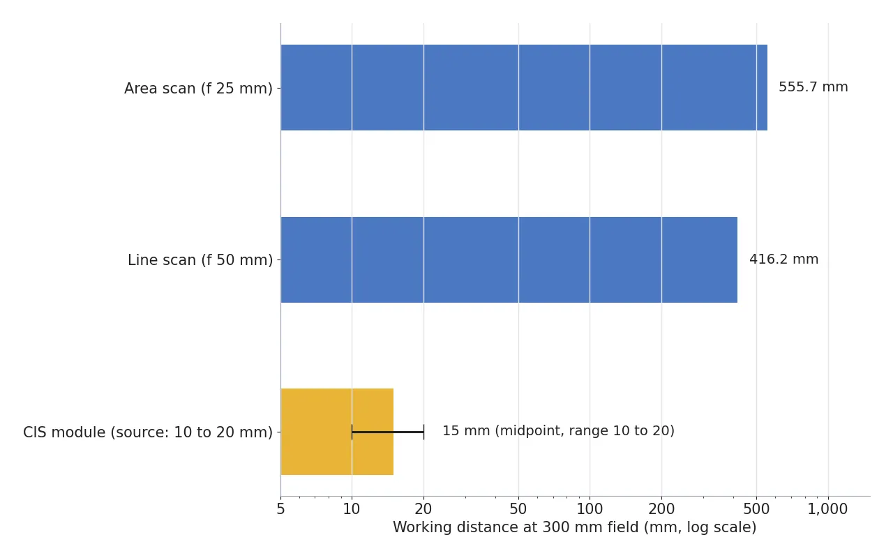
On the same 300 mm field, a CIS needs a WD of 15 mm and a line scan camera needs 416.2 mm.
Put area scan, line scan, CIS and a smart camera over one panel and calculate pixel size and WD, then the data rate, and each camera kind shows what it is for.
About 13 min read
Say a 300 mm wide PCB panel sits on the inspection stage and you are deciding how high to mount the camera over it. The panel surface is green solder mask that looks nearly matte, and I assume its reflectance1 is middling. Only the copper pads show as smooth specular patches here and there. The target is a scratch 50 μm wide, and the panel passes at 0.5 m/s. Both the size and the speed are assumptions for the calculation.
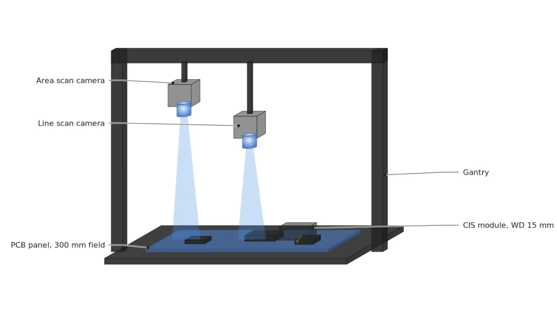
The camera kind sets that height. Area scan2 and line scan3 need a lens hung hundreds of millimeters above the panel, while a kind called CIS4 views the same 300 mm with the sensor 15 mm above it. The calculation that splits cameras by shutter, color and cable is in the article comparing camera types, and here the camera kinds are split by what the body looks like and where the decision happens. Set the height wrong and the fixture gets rebuilt, and a missed scratch ships in a good-parts box. With four kinds over one panel, the question is which one gets how close and sees how finely.
Camera kinds split first by sensor shape and lens distance
Three criteria separate the camera kinds: whether the sensor is a line or an area, whether the lens is mounted separately, and whether the decision sits inside the camera. Area scan puts a separate lens on an area sensor and takes one picture, and line scan stacks lines from a one-row sensor as the sample passes. According to Vision Systems, a CIS is a module that packs several line sensors, optics on the chip and a light source into one body, and a smart camera5 is a device that packs the sensor, the decision and the inputs and outputs into one body. I ask these three questions in that order when choosing a camera.
3D and infrared cameras read different physical quantities, and they are calculated separately in the article comparing vision types. Here only the four kinds that view the same surface in visible light go over the panel.
Area and line scan cut the same 300 mm in different ways
Assume the area scan camera has 4,096 px across, 3.45 μm pixels and a 25 mm lens. Dividing the 300 mm field into 4,096 pixels gives 73.24 μm each, the 14.13 mm sensor width gives a magnification of 0.047, and the WD6 is 25 mm × (1 + 1 ÷ 0.047) = 555.7 mm. A 50 μm scratch covers 0.68 pixel and does not fill even one.
Assume the line scan camera has 8,192 px, 5 μm pixels and a 50 mm lens, and one pixel is 36.62 μm with a WD of 416.2 mm. The 50 μm scratch covers 1.37 pixels, better than area scan but short of two. With the panel passing at 0.5 m/s the line rate is 0.5 m/s ÷ 36.62 μm = 13.65 kHz, and one line gets 73.2 μs of exposure or less. Vision Systems explains that a conventional line scan with a reducing lens needs a distance comparable to the object width, and this calculation agrees: a 300 mm width comes with a 416.2 mm WD.
To hold 50 μm at two pixels or more, both kinds have to shrink the field and shoot it in several passes. With one lens, the distance from lens to panel grows with the field width, and that is the problem. I start by looking for a way to shorten that distance, and the answer is the CIS.
The CIS puts the lens and the light next to the sensor
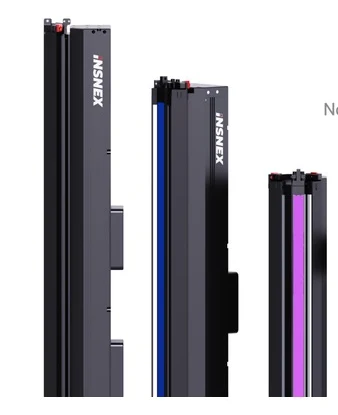
A CIS sets graded-index lenses7 in a row to make one line of magnifiers. In Vision Systems, each lens images only a narrow stretch and the images of neighboring lenses overlap into one sharp line. The light is a long LED line or a fluorescent tube built into the module. Quality Magazine says the lens magnification is 1:1 and the WD is typically 10 to 20 mm, against 250 to 500 mm for a conventional line scan system. The 416.2 mm line scan figure calculated above falls inside that range.
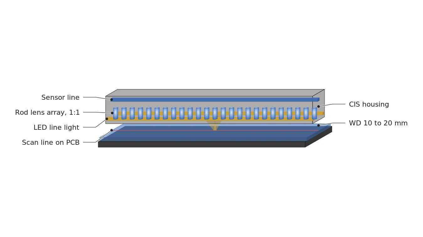
Look first at the gap between the sensor line and the red line on the panel. Two yellow LED rows gather light toward the center, and the lens carries only that red line onto the sensor line at 1:1. The 15 mm gap (the midpoint of the 10 to 20 mm range) is drawn to the same scale, and the module looks as if it touches the panel. Against line scan it is 416.2 mm ÷ 15 mm = 27.7 times closer, and against area scan 555.7 mm ÷ 15 mm = 37.0 times.
Pixel size is read in dpi8. At 600 dpi, which Quality Magazine calls common, one pixel is 25.4 mm ÷ 600 = 42.33 μm, and at 900 dpi it is 28.22 μm. Across 300 mm that is 10,630 pixels at 900 dpi and 7,087 at 600 dpi. The 50 μm scratch covers 1.77 pixels at 900 dpi and 1.18 at 600 dpi. The same source compares MTF (40.9 % against 27.6 % on a 45 μm line target), which confirms that smaller pixels keep thinner lines.
A CIS comes with conditions. The two sources give no depth of field figure, but the B2S product list shows the INSNEX LX2 900 dpi model with Accuracy 28.2 μm, WD 15 mm, Depth of Field ±1.3 mm and Interface 10GigE. That is one model, so whether the height variation of the panel top stays within ±1.3 mm is an item to confirm in the data sheet of the module you plan to use. How the built-in LED line light responds over the specular copper pads cannot be guaranteed before a sample test. Quality Magazine recommends an IP60 rating because the short WD lets dust reach the optical path, and names speed and resolution as the present limits. It also notes that modules built from butted chips leave gaps with missing pixels.
Where one CIS line passes 1 Gb/s
Smaller pixels make lines read faster on a panel passing at the same speed. At 900 dpi the rate is 0.5 m/s ÷ 28.22 μm = 17.72 kHz, and one line gets 56.4 μs of exposure or less. A line holds 10,630 px, so at 8 bit it is 10,630 × 8 bit × 17.72 kHz = 1.51 Gb/s. At 600 dpi it is 11.81 kHz and 0.67 Gb/s, and the line scan camera above is 13.65 kHz with 8,192 × 8 bit, or 0.895 Gb/s.
28.2μm
One pixel at CIS 900 dpi (10,630 px over 300 mm)
15mm
CIS WD (midpoint of the 10 to 20 mm in the source)
1.51Gb/s
Data rate at CIS 900 dpi (8 bit, 0.5 m/s)
The third number decides the cable. In the Edmund Optics table the nominal rate of GigE is 1 Gb/s, so 900 dpi runs short of bandwidth9 while 600 dpi and line scan fit inside the nominal rate. The effective rate is lower because of overhead, so the real margin is an item to confirm in the data sheet. Quality Magazine describes Camera Link HS over fiber for CIS modules, 2.4 gigapixels per second per cable up to 300 m. The 188 Mpx/s of this calculation sits far below that.
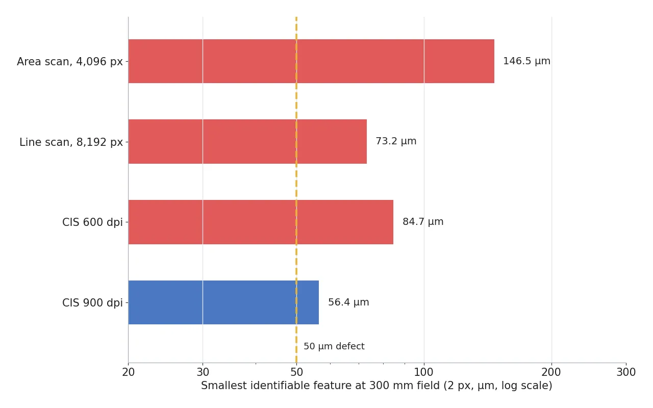
Look first at the distance between the yellow 50 μm dashed line and the end of each bar. With a two-pixel criterion the smallest identifiable size is 146.5 μm for area scan, 73.2 μm for line scan, 84.7 μm for CIS 600 dpi and 56.4 μm for CIS 900 dpi, so the bar that comes closest to the line is CIS 900 dpi. My standard is two pixels, so even that bar stays short of passing. To catch this panel’s scratch reliably the field has to be divided, or a module with smaller pixels used.
Smart cameras put the decision inside the camera
A smart camera packs the sensor, the decision and the inputs and outputs into one body. An article on automate.org that collects industry opinions defines a smart camera as a self-contained unit with the imager plus the intelligence and the I/O, and says it is also called a vision sensor. In the same article a PC-based system takes several camera inputs and can be expanded, while a smart camera has a fixed performance envelope.
Cost runs the other way. One expert in the same article says smart cameras are generally cheaper to buy and set up because the camera, the lens and the lighting come bundled with the cabling and the processing. They suit fixed-scope jobs such as presence checks and barcode reading, and the opinion that a PC fits better once the computation gets heavy follows. The article dates from 2002, so its speed and resolution figures are not carried over and only its way of dividing the kinds is borrowed. How far a current smart camera goes is an item to confirm in each model’s data sheet.
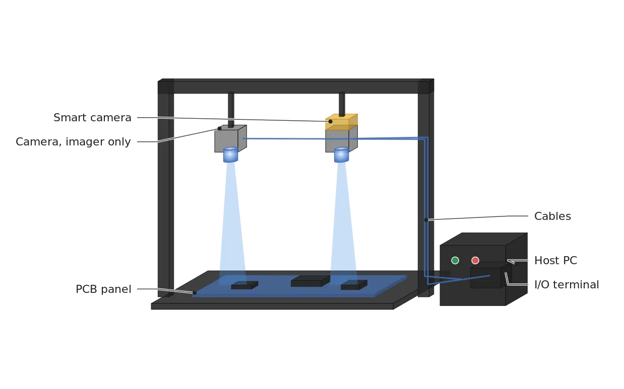
Look first at where the cables go. The cable of the imager-only camera (left) runs to a host PC, and the cable of the smart camera (right), with a yellow processor on top, ends at a small I/O terminal. Both cameras are drawn at the area scan WD of 555.7 mm, though the real sensor and lens of a smart camera are values to confirm in each model’s data sheet. I hand a smart camera the jobs with a fixed scope first.
Five rows on one data sheet
Same panel, same speed, read one row at a time. The assumed values are those stated in the earlier sections, and changing the sensor resolution or the lens means recalculating each row. The smart camera row has nothing to calculate, so only items to confirm are written.
| Camera kind | ① Smallest identifiable size | ② Optical setup · WD | ③ Algorithm parameters · In plain words |
|---|---|---|---|
| Area scan | 146.5 μm (2 px, 73.24 μm/px). 50 μm is 0.68 px | 25 mm lens, WD 555.7 mm (confirm in the data sheet), dome light | The field has to be split into several shots. It takes the whole picture at once but the pixel is large |
| Line scan | 73.2 μm (2 px, 36.62 μm/px). 50 μm is 1.37 px | 50 mm lens, WD 416.2 mm, line light | Encoder division 1 line = 36.62 μm, line rate 13.65 kHz, exposure 73.2 μs or less, 0.895 Gb/s. It stacks lines into one picture |
| CIS 900 dpi | 56.4 μm (2 px, 28.22 μm/px). 50 μm is 1.77 px | Lens and LED built in, WD 10 to 20 mm (Quality Magazine), IP60 recommended for the optical path | Line rate 17.72 kHz, exposure 56.4 μs or less, 1.51 Gb/s which exceeds the nominal 1 Gb/s of GigE. It reads with the module pressed close to the panel |
| CIS 600 dpi | 84.7 μm (2 px, 42.33 μm/px). 50 μm is 1.18 px | Lens and LED built in, WD 10 to 20 mm | Line rate 11.81 kHz, exposure 84.7 μs or less, 0.67 Gb/s. Lower cost and slightly larger pixels |
| Smart camera | Confirm in the sensor data sheet | Confirm lens, lighting and WD per model | The range of decision tools and the number of I/O points are fixed. The decision sits in the same body, so the cable is short |
What shows first across the five rows is that the WD moves from 555.7 mm to 15 mm, more than two orders of magnitude, while the smallest identifiable size at two pixels shrinks from 146.5 μm to 56.4 μm, less than threefold. Moving closer shortens the distance, and the pixel size is set by the dpi of the sensor. Some conditions favor the opposite approach. If the defect is over 0.5 mm and pixel size does not matter, or the panel warps so that a 15 mm gap cannot be kept, an area or line scan with a separate lens is better. When the assumed values in the table are replaced by real specifications, every row must be recalculated, and the result cannot be guaranteed before a sample test.
Which camera goes up first, and who pays
The order is short. Work out the pixels needed from the field width and the defect size, check how much height there is over the panel for a camera, then decide the data rate and where the decision sits. In my own data sheet I would put the micrometers per pixel and the WD on the first line in place of a model name. If you are starting out, I recommend doing by hand the calculation of dividing the field by the pixel count.
The job that makes this choice is the machine vision engineer, and a person who can say how pixel size, distance and the data rate change with each camera kind finishes a conversation on site quickly. For those funding the equipment, the CIS shortens the lens distance but dust protection and cable bandwidth carry a price, and the smart camera is cheap as a bundle but its decision range is fixed. This article explains technology and is not investment advice. See our Disclaimer.
Field Note
On a new panel I measure the height variation of the top surface with a ruler before choosing a camera. A CIS sits around 15 mm away, so how many millimeters the panel warps decides whether it stays inside the depth of field of the module, and I look that figure up in the data sheet. For the copper pad spots that wash out to white, I take one picture under the built-in LED line light. I also pass the panel at 0.5 m/s and check that the line spacing stays even against the encoder signal.
Field Checkpoints
Turning height, pixel and data rate into data sheet lines leaves the following seven.
- Is the WD from lens to panel top (area scan 555.7 mm, line scan 416.2 mm, CIS 10 to 20 mm) still secured after adding the fixture and the lighting? (does the warp of the panel stay inside the CIS gap)
- Does the 50 μm scratch cover at least two pixels? (CIS 900 dpi is still 1.77 px, so does the field need splitting)
- Are an encoder signal for the line rate (line scan 13.65 kHz, CIS 900 dpi 17.72 kHz) and the exposure limit (73.2 μs, 56.4 μs) secured? (is the light bright enough at that exposure)
- Does the required data rate (line scan 0.895 Gb/s, CIS 900 dpi 1.51 Gb/s) fit inside the effective rate of the chosen interface? (does it pass the nominal 1 Gb/s of GigE)
- Have the depth of field of the module you will use (one model on the B2S list gives ±1.3 mm) and the dust protection of the optical path (IP60 recommended) been checked in the data sheet? (does the short WD let dust reach it)
- If a smart camera is used, do the range of decision tools and the number of I/O points cover the requirement? (is there a way to move to a PC when the computation grows)
- Have specular spots such as copper pads and solder been checked on sample images? (the verdict waits until the calculation meets a sample)
Glossary
- [1] Reflectance reflectance
The share of the light reaching a surface that comes back off it. White paper is high and black cloth is low. ↩ - [2] Area scan area scan camera
A camera whose sensor has pixels laid out in rows and columns and takes one whole picture per shot, like a smartphone camera. ↩ - [3] Line scan line scan camera
A camera with a single row of pixels that builds a picture by stacking lines while the sample passes by. ↩ - [4] CIS contact image sensor
A module that packs a line sensor, a lens array and a light into one body and sits close to the sample. It is built like the reading bar inside a copier or scanner. ↩ - [5] Smart camera smart camera
A camera that puts the imaging sensor, a processor that makes decisions, and inputs and outputs in one body. It is also called a vision sensor. ↩ - [6] WD working distance
The distance from the lens to the top of the part being inspected. The text calculates it with a thin-lens approximation from the principal plane, and the reference plane a maker uses has to be checked in the data sheet. ↩ - [7] Graded-index lens graded-index lens
A small lens whose refractive index changes from the center of a glass rod outward and so gathers light. Set in a row, the lenses image a line at true size. ↩ - [8] dpi dots per inch
The number of pixels in one inch (25.4 mm). At 900 dpi one pixel is 25.4 mm ÷ 900 = 28.2 μm. ↩ - [9] Bandwidth bandwidth
The number of bits a cable can carry in one second. The bits the camera produces per second must stay below it. ↩
References
- Vision Systems Design, Contact image sensors challenge linescan cameras (CIS composition, graded-index lenses, 20 mm mounting distance, distance of a conventional line scan), accessed October 14, 2026
- Quality Magazine, Innovations shaping the future of contact image sensor technology (WD of 10 to 20 mm against 250 to 500 mm, 1:1 magnification, 600 and 900 dpi, MTF, interface, limits), accessed October 14, 2026
- automate.org, Smart Cameras vs. PC-Based Machine Vision Systems (definition of a smart camera, differences from PC-based, cost, uses; a 2002 article), accessed October 14, 2026
- Edmund Optics, Camera Types and Interfaces for Machine Vision Applications (nominal GigE rate), accessed October 14, 2026
- B2S, CIS Line product list (Accuracy, WD, Depth of Field and Interface of the INSNEX LX2 900 dpi model), accessed October 14, 2026
- Formulas: pixel footprint = field ÷ horizontal pixel count, magnification = sensor width ÷ field, WD = f × (1 + 1 ÷ magnification), CIS pixel = 25.4 mm ÷ dpi, line rate = sample speed ÷ pixel footprint, data rate = pixels per line × bit depth × line rate

Noctvision
An engineer who designs secondary-battery manufacturing equipment keeps this record while studying local AI on single-board computers such as the Raspberry Pi and Jetson.

You May Also Like
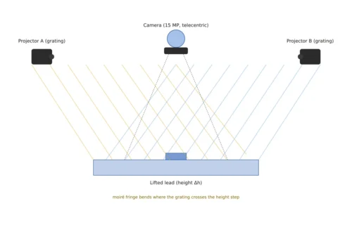
What 2D Contrast Can’t See: How 3D Structured-Light Inspection Measures Solder Joint Height
There Are Defects That Vanish in Visible Light — Inspection Design Beyond the 1 μm Barrier in SWIR Imaging