There Are Defects That Vanish in Visible Light — Inspection Design Beyond the 1 μm Barrier in SWIR Imaging
OPTICS · LIGHTING
Foreign matter inside a transparent cover, voids inside an injection-molded part, delamination between layers of a multilayer film — these three are, in principle, difficult to catch with a visible-light camera. The target material is either opaque or, conversely, fully transparent in visible light, so no absorption difference forms between the defect and the background. Where there is no contrast, no algorithm can manufacture a defect.
Leaving this condition unaddressed carries a clear cost. Internal foreign matter discovered only after assembly leads to scrapping the finished product, and interlayer defects in a multilayer film surface as functional failures only at the end-use stage. A gap opens up where passing inspection no longer guarantees quality.
The solution is not the algorithm — it is changing the wavelength. In the SWIR imaging (Short-Wave InfraRed, roughly 900–1700 nm) band, silicon, certain plastics, and water show transmission and absorption characteristics entirely different from visible light. What is opaque in visible light becomes transparent in SWIR, and two materials indistinguishable in visible light separate cleanly by absorption-band difference in SWIR.
When there is no contrast, the first thing to suspect is not the algorithm — it is wavelength selection.
SWIR is not infrared thermal imaging
Point. The most common misunderstanding in SWIR imaging inspection is treating it as the same category as thermal imaging (LWIR).
Reason. LWIR (8–14 µm) observes the radiation a target emits on its own. It therefore needs no illumination, but yields only a temperature contrast. SWIR is the opposite. Because a room-temperature object’s self-emission is negligible, SWIR-band illumination is mandatory, and in exchange you obtain a reflectance-and-transmittance image just like visible light. In other words, SWIR is, by nature, a machine-vision band where lighting design determines success or failure.
Example. Water has a distinct absorption band near 1450 nm. Because of this, wet regions appear dark in SWIR and separate clearly from dry regions of the same color. Conversely, silicon’s transmittance rises sharply above 1100 nm, opening a window into the interior of a wafer. Both phenomena are the result of choosing the illumination wavelength, not a product of any algorithm.
Point. The first line of a SWIR adoption review should not be camera specifications — it should be the target material’s SWIR-band transmission and absorption profile.
The 1 µm barrier and pixel pitch — why now
Point. The reason SWIR long remained specialized equipment was not performance — it was pixel pitch and unit cost.
Reason. SWIR detection is handled by InGaAs compound-semiconductor photodiodes, while signal readout is handled by silicon circuitry. The two chips must be bonded together, and traditional bump bonding could not shrink pixel pitch below a certain size because of bond-pad dimensions. As a result, raising resolution enlarged the sensor, and a larger sensor drove up both the optics and the unit cost in a vicious cycle.
Example. Stacked SWIR sensor technology using Cu-Cu bonding (direct copper-pad bonding) broke this constraint. Fine-pitch bonding made it possible to achieve pixel sizes close to industrial CMOS alongside megapixel-class resolution at the same time. On top of this, recent sensor families have extended their response band out to 400–1900 nm, making it possible to handle visible light and SWIR with a single sensor at once. The “1 µm barrier” refers to this continuous visible-to-SWIR response.
Point. The practical implication is clear. In the past, a visible-light camera and a SWIR camera sat at separate stations, fighting registration error; now a design is possible that captures both frames on the same optical axis, changing only the wavelength.
Lighting comes first — where SWIR setups fail
Point. Most failures in SWIR system adoption occur not in the camera, but in the lighting and the lens.
Reason. First, ordinary machine-vision lenses are coated and chromatically corrected for the visible band, so in SWIR the focus position shifts and transmittance drops. A SWIR-dedicated or VIS-SWIR apochromatic lens is required. Second, SWIR LEDs carry a higher cost per unit of optical output than visible-light LEDs, which tightens the illuminance budget. Third, in applications that require transmitted illumination (internal foreign matter, interlayer delamination), backlight uniformity directly determines the detection floor.
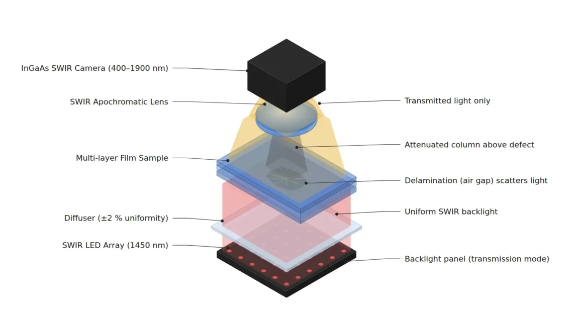
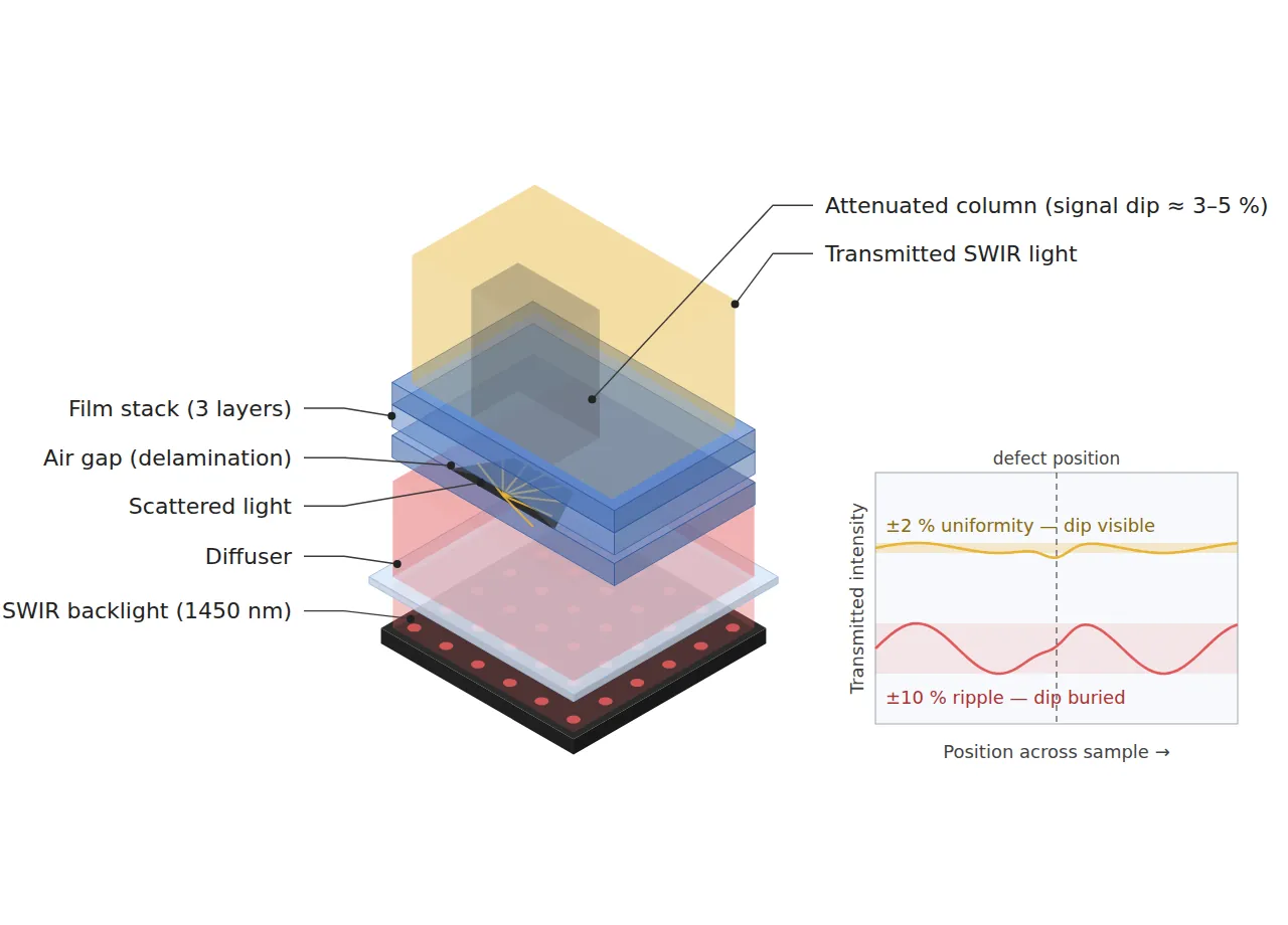
Example. Assume a delamination inspection for a multilayer packaging film. Under 1450 nm transmitted illumination, the delaminated region scatters more due to the air gap and appears darker. If backlight uniformity is ±10%, the delamination signal — typically only a few percent of transmittance difference — is buried in the uniformity variation. A uniformity of ±2% or better becomes the practical requirement.
Point. In other words, in SWIR inspection illuminance and uniformity are not a brightness issue — they are a specification that directly defines the detection floor. Software correction should not be assumed to substitute for hardware lighting uniformity.
Changing the wavelength changes what becomes visible. But if you do not change the lighting, the meaning of changing the wavelength disappears.
Core framework — minimum defect size / optical setup / algorithm matching table
| Category | Item | Spec / Parameter | Basis · Notes |
|---|---|---|---|
| ① Min. defect size | Foreign matter inside transparent cover | Minimum diameter 100 µm | Based on transmission image; requires ≥3 px occupancy |
| ① Min. defect size | Multilayer film interlayer delamination | Minimum area 500 µm x 500 µm | Assumes ~3–5% transmittance difference; requires empirical verification |
| ① Min. defect size | Residual moisture region | Minimum diameter 200 µm | Uses the 1450 nm absorption band |
| ② Optical setup | Camera | InGaAs-based SWIR sensor, ~5 MP class, pixel pitch ~5 µm | Assumes Cu-Cu bonded stacked sensor |
| ② Optical setup | Band | 900–1700 nm (wideband type: 400–1900 nm) | Choose wideband type for simultaneous visible-light acquisition |
| ② Optical setup | Lens | SWIR-compatible or VIS-SWIR apochromatic, focal length 35 mm, F/4 | Repurposing a visible-only lens is prohibited |
| ② Optical setup | WD (Working Distance) | Minimum 200 mm required | Confirm empirically against interference with the transmitted-illumination backlight structure |
| ② Optical setup | Lighting | 1450 nm transmitted backlight, uniformity within ±2% | Uniformity directly determines the detection floor |
| ② Optical setup | Magnification · FOV | FOV 120 mm x 90 mm, 33 µm/px | 100 µm foreign matter occupies 3 px |
| ③ Algorithm | Preprocessing | Flat-field correction (division by backlight profile) | Removes uniformity residuals |
| ③ Algorithm | Band operation | Two-band ratio image, 1450 nm / 1200 nm | Separates thickness variation from absorption variation |
| ③ Algorithm | Detection threshold | Local deviation of ratio image exceeding 3σ | σ re-estimated from 30 known-good samples |
| ③ Algorithm | Minimum defect area | Connected component ≥9 px | Removes single hot pixels |
Table takeaway. The ±2% lighting uniformity in ② and the 3σ detection threshold in ③ are, in effect, the same number used on both sides. If lighting uniformity is relaxed to ±5%, the 3σ threshold automatically becomes meaningless, and the moment the algorithm side raises the threshold to compensate, the 100 µm foreign-matter defect drops out of the detectable range.
Related Patents (Confirmed to Exist)
| Patent No. | Title | Assignee |
|---|---|---|
| US 11,063,079 B2 | Germanium based focal plane array for the short infrared spectral regime | TriEye Ltd. |
| US 12,100,725 B2 | Germanium based focal plane array for the short infrared spectral regime (continuation application, same family) | TriEye Ltd. |
| US 7,655,908 B2 | Enhanced vision system sensitive to infrared radiation | Teledyne FLIR, LLC (successor by merger) |
Patents whose assignee could not be explicitly confirmed were excluded from citation.
Conditions Favoring the Opposite Approach
- When the defect is confined to surface topography (scratches, dents): SWIR’s transmission advantage does not apply, so visible-light angled illumination or a deflectometry method is favorable.
- When securing sufficient light is difficult on a high-speed line: the per-unit cost and output limits of SWIR illumination make exposure time the bottleneck. If there is even a slight possibility of creating contrast in the visible band, that route is more economical.
- When the target is a material combination that shows no absorption difference in the SWIR band: changing the wavelength yields nothing.
SWIR transmission and absorption characteristics vary greatly by material additive, pigment, and thickness, so this cannot be confirmed before sample testing.
Field Checkpoints
- Is a WD of 200 mm or more confirmed by measurement? — Check including the transmitted-illumination backlight housing and the transport mechanism.
- Has the target material’s SWIR-band transmission spectrum been measured? — Confirm with actual lot samples, not generic resin values from a datasheet.
- Is the lens a product validated for the SWIR band? — Using a visible-only lens causes focus shift and transmittance loss at the same time.
- Has backlight uniformity been measured to within ±2%? — Measure against the raw baseline before flat-field correction.
- For a simultaneous visible-SWIR acquisition configuration, has the focus-position difference between the two wavelengths been checked?


You May Also Like
2D/3D Fusion Inspection: The Bottleneck Is Lighting Interference
Software-Defined Lighting: One Head, Switching Between Dark-Field and Coaxial Illumination