Where Do Fine Defects Go When You Shrink to 640 × 640? — Overlap, Boundary and Latency Design for Edge AI Tiled Inference
EDGE AI / ALGORITHM
Most detection models for edge devices are trained and deployed at a fixed input resolution of around 640 × 640 px. Inspection cameras, on the other hand, output high-resolution images in the 20 MP class. The gap between these two numbers is often handled with “one line of resize”: a 5472 × 3648 px image is shrunk to a width of 640 px and fed to the model.
That single line changes the entire detection floor. A 90 µm particle that occupied 3 px in the original image falls below even 1 px after downsampling, and as it is averaged with its neighboring pixels, its contrast is diluted as well. The model accuracy metric looks good, driven mostly by large defects, while only the fine defects drop out quietly, and the escapes come back as defects on the customer side. Retraining the model does not restore information that is no longer present in the input.
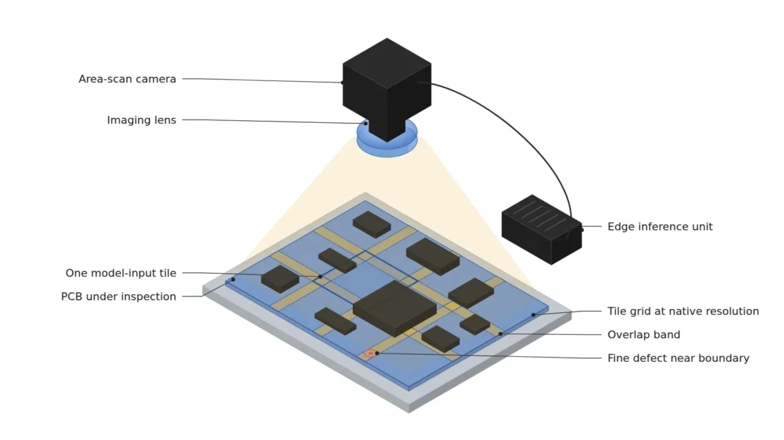
The solution, instead of shrinking the image, is tiled (split) inference that cuts the original-resolution image into model-input-sized pieces and runs inference several times. Tiling is not free, however. How to handle defects that straddle tile boundaries, how much overlap to use, and how much the increased tile count adds to inference latency must all be designed together.
Downsampling may not make a defect smaller; it may be an operation that erases it from the input.
1. Shrinking to 640 px Erases the Pixel Footprint of Fine Defects
Point. The model input resolution is in effect the pixel resolution of the inspection system, and the detection floor rises by the downsampling factor.
Reason. Pixel resolution is FOV ÷ number of pixels. Even if the optics deliver 30 µm/px, if the image the model sees is 640 px wide, the resolution from the model’s point of view is FOV ÷ 640. Moreover, downsampling usually averages several original pixels, so a defect that has become smaller than one pixel has its contrast diluted by its area ratio. It is a double loss in which size and contrast shrink at the same time.
Example. Capturing a 164 mm wide FOV with 5472 px gives about 30 µm/px, and a 90 µm solder bridge occupies 3 px. Shrinking the same image to 640 px wide gives 164 ÷ 640 ≈ 256 µm/px, and the same defect shrinks to about 0.35 px. Assuming area averaging, the fraction of one pixel’s area that the defect occupies is (90 ÷ 256)2 ≈ 0.12, so only about 12 % of the original contrast remains. To occupy 3 px in this configuration, a defect must be about 768 µm or larger.
Point. The question “down to how many µm does this model detect” must therefore be answered first not by model architecture but by µm/px at the model input.
2. Tile Overlap and Boundary Defects — The Center-Ownership Rule
Point. The quality of tiling is decided less by tile size than by how boundaries are handled.
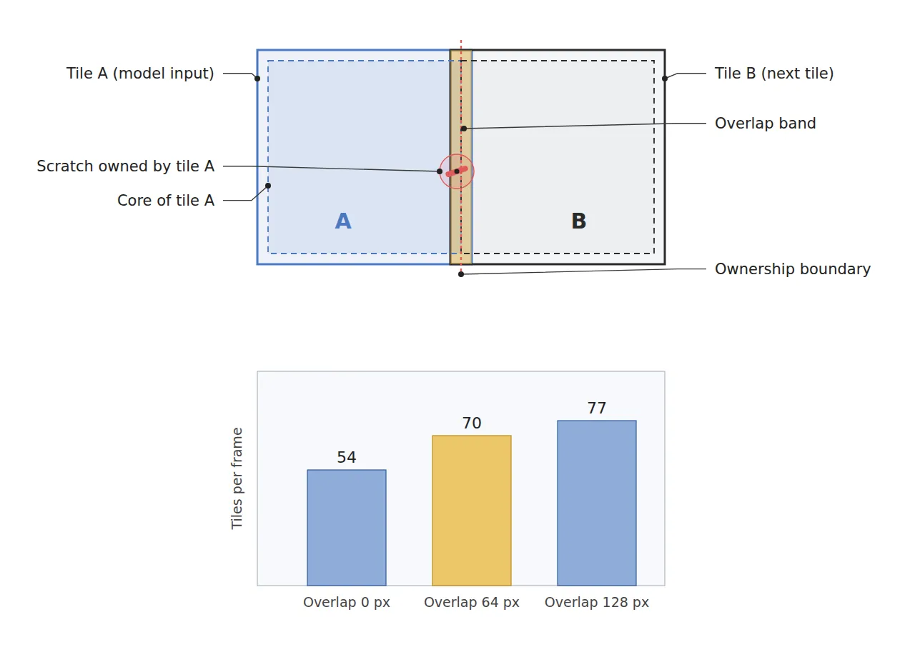
Reason. Cutting into a grid with no overlap splits a defect that straddles a boundary into two halves in two tiles. A half defect loses its shape features, its score drops, and it can be missed in both tiles. In addition, a convolutional neural network’s features weaken at the tile edges because of padding effects, so decisions near the edges are less reliable than in the center. Overlap is the device that handles both problems at once.
Example. A rule that works well in practice is the combination of overlap ≥ maximum defect size (px) and the center-ownership rule. With an overlap of 64 px, the interior of each tile excluding its outer 32 px becomes that tile’s “core”, and the cores divide the frame without gaps. Each tile keeps only detections whose box center lies inside its own core. A 1,500 µm scratch is 50 px at 30 µm/px, so if its center is inside the core it needs at most 25 px to the edge, which fits within the 32 px margin. The whole defect is seen intact within one tile and is counted only once. After that, per-class NMS (IoU 0.5) cleans up only the residual duplicates.
Point. Boundary handling should be approached not as “erase duplicate boxes with NMS” but as a design that gives ownership of each defect to the one tile in which it is seen intact.
3. The Trade Between Tile Count and Inference Latency
Point. Tiling recovers resolution in exchange for multiplying the number of inferences, and the bill for that cost is paid in line takt.
Reason. The number of tiles along one axis is roughly “(image width − tile width) ÷ stride + 1”, where the stride is the tile width minus the overlap. Increasing the overlap shortens the stride and raises the tile count along both axes together, so the amount of computation grows close to the square with respect to the overlap ratio. Unlike servers, edge devices find it hard to raise throughput with large batches, so the tile count turns almost directly into latency.
Example. Cutting a 5472 × 3648 px image into 640 × 640 tiles gives 9 × 6 = 54 tiles with no overlap, 10 × 7 = 70 tiles with a 64 px overlap (stride 576), and 11 × 7 = 77 tiles with a 128 px overlap. At 8 ms per tile (INT8 quantization, design assumption), sequential inference alone takes 560 ms for the 64 px overlap configuration. If the takt is 400 ms, it does not fit. This is where a two-stage structure helps. One inference on the whole image shrunk to 640 px checks large defects such as missing components, and for fine defects only about 28 tiles covering the CAD-defined pad and component areas (about 40 % of the frame, design assumption) are inferred at original resolution. The total is about 8 + 224 = 232 ms.
Point. The starting point of tiling design is not the model but a process map of “which defects of which size appear in which areas”. Running original-resolution inference on areas where fine defects cannot occur only consumes takt.
4. Core Framework — Matching Table
| Category | Item | Specification / Parameter | Basis & Notes |
|---|---|---|---|
| ① Minimum defect size | Solder bridge & fine particle | 90 µm or more | Design assumption. 3 px at original resolution, about 0.35 px after 640 px downsampling |
| ① Minimum defect size | Pad scratch (basis for overlap sizing) | Length up to 1,500 µm | Design assumption. About 50 px, not more than the 64 px overlap |
| ① Minimum defect size | Missing or skewed component | 1,000 µm or more | Design assumption. About 3.9 px at 256 µm/px on the downsampled path |
| ② Optical setup | Illumination & target material | Diffuse dome light, PCB substrate and solder joints | Solder mixes high and diffuse reflection; cannot be confirmed before sample testing |
| ② Optical setup | Camera | 20 MP, 5472 × 3648 px, 2.4 µm pixel | Sensor about 13.1 mm × 8.8 mm |
| ② Optical setup | Lens | Focal length 35 mm, magnification about 0.080 | Design assumption |
| ② Optical setup | WD (working distance) | 450 mm or more must be secured | Thin-lens object distance about 472 mm. Measure including dome light height and aperture |
| ② Optical setup | FOV & pixel resolution | 164 mm × 109 mm, about 30 µm/px | 164 ÷ 5472 ≈ 29.97, 109 ÷ 3648 ≈ 29.88 |
| ③ Algorithm | Tile split | 640 × 640 px, 64 px overlap (stride 576) → 10 × 7 = 70 tiles | 54 tiles with no overlap, about 1.30 times |
| ③ Algorithm | Boundary merge | Center-ownership rule (core excludes outer 32 px) + per-class NMS IoU 0.5 | Defect half-length 25 px ≤ 32 px |
| ③ Algorithm | Inference latency | 8 ms per tile (INT8) → full tiling 560 ms sequential | Design assumption. Exceeds 400 ms takt |
| ③ Algorithm | Two-stage structure | One whole-image 640 px pass + about 28 CAD ROI tiles → about 232 ms | Assumes ROI area of about 40 % |
Table implication. A 90 µm defect that occupies 3 px at the original 30 µm/px disappears to 0.35 px on the 640 px downsampled path (256 µm/px), while a 1,000 µm missing component keeps about 3.9 px even on that same path. In other words, splitting paths by defect size is justified, and a 64 px overlap is the choice that covers the 50 px maximum defect while holding the tile count increase to 1.30 times. The calculation that full tiling at 560 ms exceeds the 400 ms takt is the direct basis for requiring the two-stage structure.
5. When the Opposite Approach Wins
- When all defects are large and global context matters: If the targets are only defects of about 768 µm or more, such as missing components or reversed polarity, a single whole-image inference is fast and has no boundary problems.
- When there is ample compute headroom: Running a model with a larger input resolution once can be simpler than maintaining tile merge logic. However, computation grows close to the square of the input side length.
- When the FOV can be split optically: Capturing a narrow FOV from the start with a higher-magnification lens or multiple cameras secures resolution without software splitting. Hardware cost and WD interference review follow.
On surfaces where specular and diffuse reflection mix, such as solder joints, defect contrast depends heavily on illumination angle, and detection can vary even at the tile’s original resolution, so this cannot be confirmed before sample testing.
Field Note
In PCB appearance inspection on a high-speed assembly line, I once started with a configuration that shrank the whole image to 640 px. The overall metrics on the validation set were fine, but recall was unusually low only for particles of around 100 µm, and when I enlarged the input image, the defects remained only as faint smudges one or two pixels wide. After switching to tiling, the problem of the same defect being caught twice at boundaries followed, which was resolved by setting the overlap to 64 px and adding the center-ownership rule. Even so, sequential inference latency exceeded the takt, and as I recall we eventually moved to a two-stage structure that views only the CAD-based ROI at original resolution.
Field Checkpoints
- Is a WD of 450 mm or more secured by measurement — verify including the dome light height and the camera aperture position.
- Has the surface material and reflectance of the target been confirmed first — specular reflection from solder and gold-plated pads governs defect contrast.
- Does the minimum defect occupy 3 px or more at the model input µm/px.
- Is the overlap at least the maximum defect size (px), and does the center-ownership rule block double counting.
- Does tile count × per-tile latency fit within the line takt — if not, consider an ROI-based two-stage structure.
- Have validation metrics been checked separately by defect size range — the overall average hides missed fine defects.

Noctvision
A machine vision engineer who fits cameras, lenses, lighting, and image-processing algorithms together for a living. Years spent on continuous production lines, vibration, heat, and dust included, working through diffuse reflection, contrast, and resolution differences too fine for a spec sheet to capture inform every post here, closing the gap between theory and the shop floor. Off duty, that same eye for light and lenses goes into repairing fully mechanical vintage film cameras.


You May Also Like
AOI Only Says “Defective” — How Vision Language Models Fill the Gap in Judgment Rationale
Does Extending the Exposure Solve It When Light Is Short? — How SPAD Sensors and Time Gating Rewrite Low-Light Inspection Design