Does Extending the Exposure Solve It When Light Is Short? — How SPAD Sensors and Time Gating Rewrite Low-Light Inspection Design
OPTICS / EDGE AI
Sites short on inspection light share a common response pattern. Extend the exposure time, raise the gain, and swap the illumination for something one step brighter. All three demand a price in line speed, damage to the target, or heat. And all three fail to touch the root problem — when few photons reach the detector, the accuracy of counting those few photons degrades.
Left unaddressed, the cost shows up at the detection floor. Brightness gained by extending the exposure also creates motion blur, and signal gained by raising the gain amplifies read noise along with it. In the end, fine defects on the order of tens of µm fall below the noise floor and pass. A section appears where only the record of having gone through inspection remains, while quality is not guaranteed.
The direction of the solution is not “brighter” but “switch to a detector that counts single photons, and choose the time interval in which to count”. A single-photon avalanche diode (SPAD) amplifies the electron created by one photon into an avalanche and converts it into a digital pulse. Unlike a conventional CMOS that integrates analog charge, read noise does not intervene in principle. Add programmable time gating on top, and a new contrast axis opens up — sorting photons by their arrival time.
When there is no contrast, the last remaining axis is not brightness but the arrival time of the photon.
1. A SPAD Sensor Is Not a “High-Sensitivity Camera”
Point. Understanding a SPAD sensor simply as a “camera strong in low light” sends the deployment design off course.
Reason. A conventional CMOS pixel collects charge during the exposure interval and reads it out as a voltage at the end. Read noise is added during this readout, and the smaller the signal, the larger the noise share. A SPAD pixel is different. When a single photon triggers avalanche breakdown, that alone produces a saturation-level digital pulse. The measured quantity is not the charge but the number of pulses, and the noise comes not from the readout circuit but from the statistical fluctuation of photon arrival (shot noise) and the dark count. In other words, a SPAD sensor is not an analog brightness meter but a digital counter.
Example. In September 2026, Singular Photonics of Edinburgh launched the SPAD image sensor Litavis. According to the company, it is the first SPAD sensor to unify imaging, timing, histogramming and photon statistics on one chip through in-pixel processing. It provides continuous 256 × 256 px photon-counting imaging under low-light conditions and, at the same time, generates picosecond-resolution time-stamped photon events on a 64 × 64 macropixel grid. The core of this architecture is that intensity, timing and histogram modes operate simultaneously.
Point. The first line of the design review should not be “how many lx are needed” but “how many photons arrive per pixel in a unit exposure interval”. If that question cannot be answered, the benefit of a SPAD sensor cannot be calculated.
2. Time Gating — The Axis That Cuts Scattered Light by Time
Point. What is genuinely new about a SPAD sensor is not sensitivity but the right to choose on the time axis.
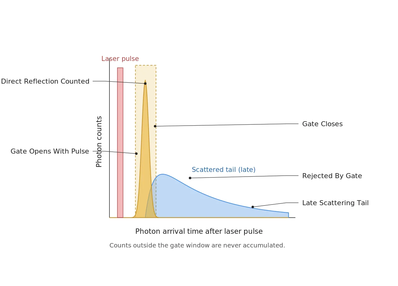
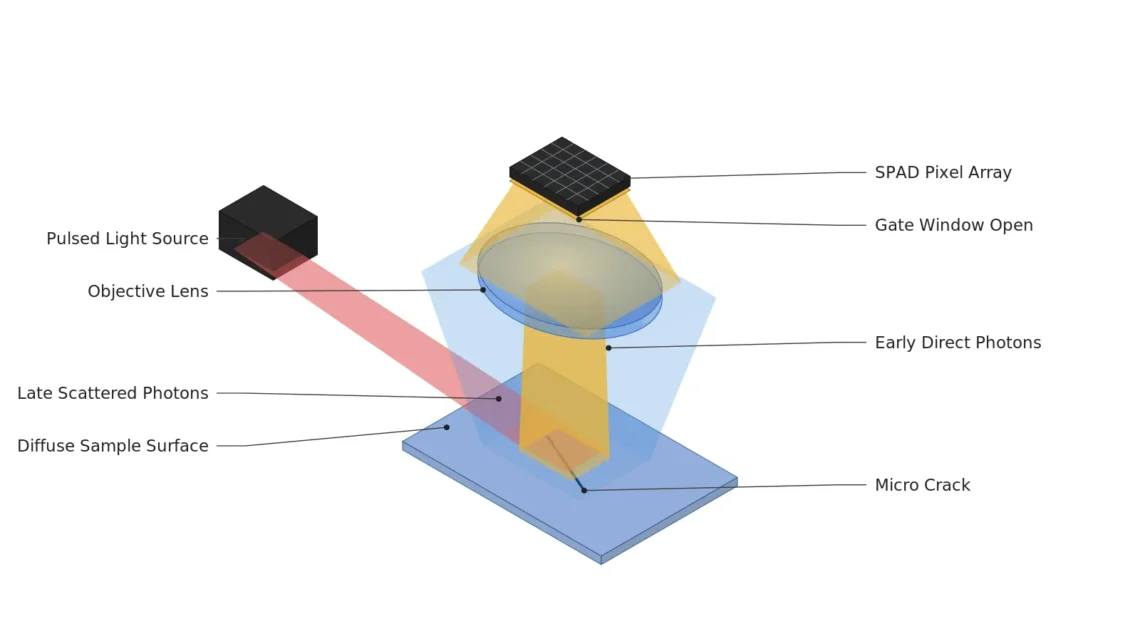
Reason. With pulsed illumination, photons reflected directly from the target surface and scattered photons that arrive late after multiple passes inside the medium have different arrival times. A conventional sensor integrates the entire exposure interval, so the two are mixed into one pixel value. Once mixed, no post-processing separates them completely. If instead the gate is opened only in a narrow interval right after the illumination pulse, the late-arriving scattering component is never counted in the first place. It is a structure in which contrast is not restored by software but created by the hardware from the outset.
Example. Consider a fine crack under a translucent resin cover. When multiple scattering inside the cover blankets the background in haze, the edge contrast of the crack collapses. Narrowing the gate width so that only the surface direct-reflection component is counted reduces the contribution of background scattering and raises edge contrast at the same illumination output. However, the magnitude of this effect depends entirely on the scattering coefficient and thickness of the material, so it cannot be guaranteed before a sample test.
Point. Time gating is a tool of the same family as an optical filter or a polarizer — in the sense that it discards unwanted light components before detection. One should not assume that software image processing can cover defects in the hardware optical setup.
3. How On-Chip Processing Changes the Data Path
Point. If photon-level events are sent outside as they are, bandwidth collapses first.
Reason. Photon events are a stream, not frames. If time-stamped events per pixel are transmitted in raw form, the data volume explodes in proportion to illumination intensity and host-side preprocessing becomes the bottleneck. That is why recent SPAD architectures finish histogram generation and photon statistics near the pixel. Singular Photonics explains that processing photon events directly on chip reduces the amount of raw data that must be transferred to external processing hardware, and that this helps lower latency and power consumption while bringing real-time decisions forward.
Example. This design direction is observed in the same form in other product lines disclosed this week. IDS is preparing the uEye Live family, which brings neural network processing closer to the camera, and LUCID is releasing the Triton Smart camera with support for open-source AI tools. Both cases point in the direction of “reduce the information near the sensor before sending it out” rather than “pull it from the sensor and decide on the host”.
Point. There is one practical insight to take from this. A SPAD sensor review is an optical review and, at the same time, a data path review. Halving the gate width roughly halves the count as well, lowering the required bandwidth, but obtaining the same statistical confidence requires increasing the number of accumulated frames, so the effective cycle time may in fact grow. If this trade relation is not calculated first, the line takt blocks you after deployment.
In a sensor that counts photons, exposure time becomes not a “brightness parameter” but a statistical sample-count parameter.
4. Core Framework — Matching Table
| Category | Item | Specification / Parameter | Basis & Notes |
|---|---|---|---|
| ① Minimum defect size | Fine crack under translucent resin cover | Width 30 µm or more | Design assumption. Presumes edge contrast secured after gating |
| ① Minimum defect size | Shallow scratch on low-reflectance matte surface | Length 200 µm or more | Design assumption. Based on 30 accumulated count frames |
| ① Minimum defect size | Fine foreign particle (low-light section) | Diameter 50 µm or more | Design assumption. Must occupy 3 px or more |
| ② Optical setup | Sensor | SPAD photon-counting imaging 256 × 256 px | Litavis published specification (not measured; manufacturer figure) |
| ② Optical setup | Timing channel | 64 × 64 macropixels, picosecond-resolution time stamps | Same source. Intensity and timing operate simultaneously |
| ② Optical setup | Illumination | Pulse-driven light source, synchronized with the gate | Gate open width determined by per-material measurement |
| ② Optical setup | Lens | Focal length 25 mm, F/2.0 or faster recommended | Design assumption. Fast lens prioritized to secure counts |
| ② Optical setup | WD (working distance) | 150 mm or more must be secured | Verify by measurement including pulse source housing and gate sync wiring interference |
| ② Optical setup | Magnification & FOV | FOV 40 mm × 40 mm, 156 µm/px | Converted on a 256 px basis. Detecting a 50 µm particle requires reducing the FOV |
| ③ Algorithm | Accumulation | 30 photon-counting frames accumulated | Presumes shot noise reduction by √N |
| ③ Algorithm | Gate scan | Sweep the gate delay in N steps to acquire the time profile | Number of steps determined by the scattering characteristics of the material |
| ③ Algorithm | Dark count correction | Subtract a per-pixel count map taken with the illumination off | SPAD-specific item. Re-acquire when temperature changes |
| ③ Algorithm | Detection threshold | Count deviation > 3σ (against the expected fluctuation based on √N) | σ re-estimated from 30 good-part images |
Table implication. At the FOV of 40 mm × 40 mm in ②, the pixel resolution is 156 µm/px, so the 50 µm particle in ① is not detectable in principle in this configuration. The resolution of 256 × 256 px is the practical constraint on adopting a SPAD sensor, and pulling the detection floor down to the µm level first requires accepting the design trade of reducing the FOV and increasing the number of stations.
5. Related Patents (Verified as Existing)
| Patent number | Title | Assignee | Priority date / Status |
|---|---|---|---|
| US 10,620,300 B2 | SPAD array with gated histogram construction | Apple Inc. | 2015-08-20 / Active |
| US 10,801,886 B2 | SPAD detector having modulated sensitivity | Apple Inc. | 2017-01-25 / Active |
Patents whose assignee could not be explicitly confirmed were excluded from citation. In particular, gated histogram construction and sensitivity modulation are prior-art areas that correspond directly to the gate scan item in ③ of the matching table above, so if an in-house implementation is under review, the scope of the claims must be checked separately.
6. Conditions Where the Opposite Approach Is Favorable
- General illumination environments with sufficient light: When photons are abundant, the counting scheme of a SPAD is instead vulnerable to saturation (count loss due to pulse pile-up). A conventional CMOS global shutter is favorable in both resolution and cost.
- Cases where high resolution is the top priority: The currently published SPAD photon-counting imaging resolution is on the order of 256 × 256 px. If a resolution of several MP is required, this is not the right target.
- Opaque diffuse surfaces with almost no scattering component: There is no component to cut on the time axis, so the gain from time gating disappears. Angular illumination or polarization is more economical.
The scattering time profile of each material depends heavily on additives, thickness and surface roughness, so it cannot be guaranteed before a sample test.
Field Note
Field Note: On a continuous strip line handling a low-light section, I’ve measured firsthand the paradox where narrowing the gate width to cut counts ends up stretching the line takt instead of shortening it. There was a run where trusting the initial design values and skipping the gate sweep cost us — the material’s actual scattering behavior didn’t match the assumption, and the accumulated frame count had to be re-tuned on the floor. It’s a concrete reminder that photon counting is clean in theory, but the scattering coefficient per material still has to be confirmed with a sample test.
Field Checkpoints
- Is a WD of 150 mm or more secured by measurement — verify including the pulse source housing and the gate sync wiring.
- Has the surface material and reflectance of the target been identified first — the gate gain differs depending on whether it is diffuse reflection or whether diffuse reflection is mixed in.
- Has the expected photon count per pixel been calculated from illumination output, exposure and aperture — the lx value alone cannot estimate counting statistics.
- Is the FOV one in which the target defect occupies 3 px or more at 256 × 256 px resolution — if not, consider splitting into multiple stations.
- Has the dark count correction map been acquired at the operating temperature — SPAD dark counts have a strong temperature dependence.
- Does the increase in accumulated frames caused by narrowing the gate width fit within the line takt.

Noctvision
A machine vision engineer who fits cameras, lenses, lighting, and image-processing algorithms together for a living. Years spent on continuous production lines, vibration, heat, and dust included, working through diffuse reflection, contrast, and resolution differences too fine for a spec sheet to capture inform every post here, closing the gap between theory and the shop floor. Off duty, that same eye for light and lenses goes into repairing fully mechanical vintage film cameras.

You May Also Like
Where Do Fine Defects Go When You Shrink to 640 × 640? — Overlap, Boundary and Latency Design for Edge AI Tiled Inference

Automotive Part Appearance Inspection: Lighting Design Comes First