What 2D Contrast Can’t See: How 3D Structured-Light Inspection Measures Solder Joint Height
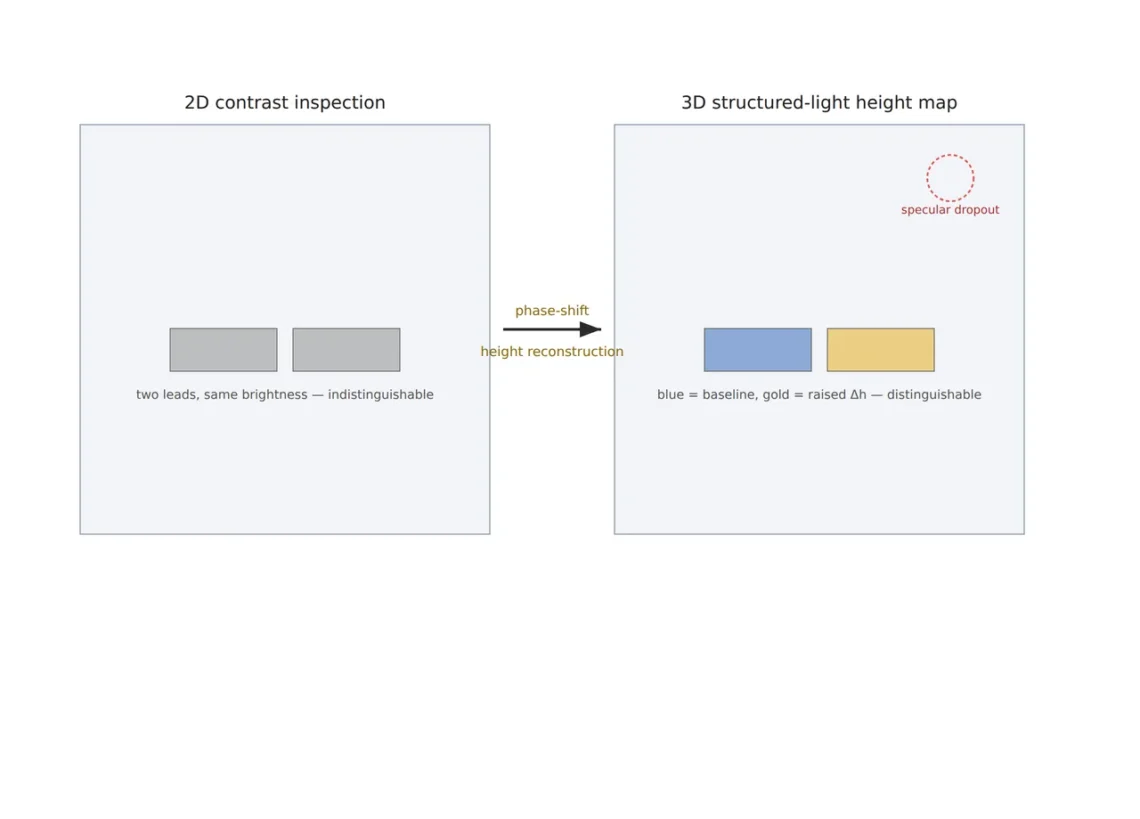
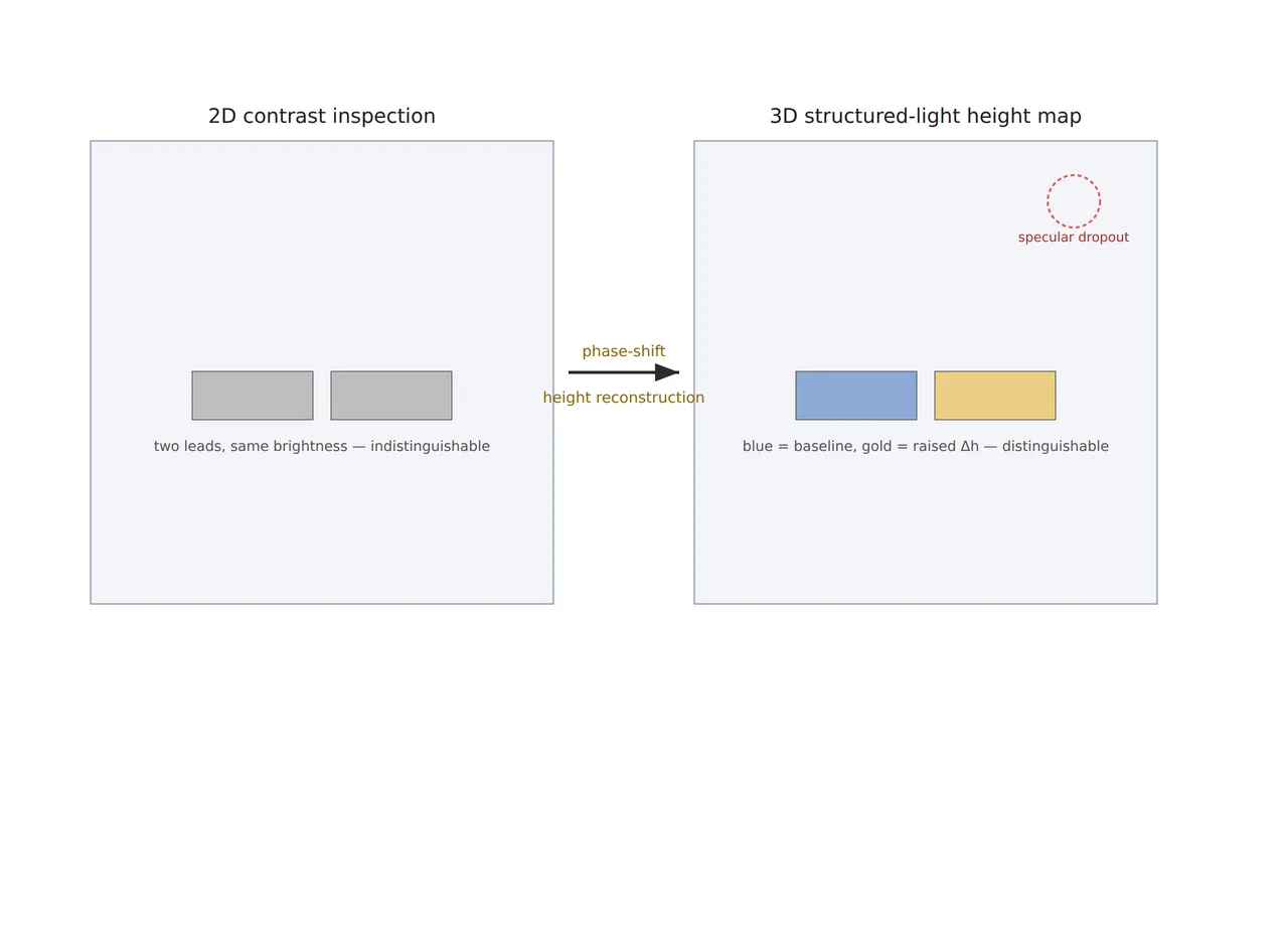
There are cases where two connector leads that passed through the same reflow line appear almost identical in color and brightness in a 2D image. One is seated normally on its pad, and the other has a slightly lifted lead — yet what a 2D camera actually sees is ultimately just the brightness and color distribution of reflected light, making the two states hard to distinguish. No matter how precisely the lighting angle is tuned, contrast-based judgment is strong for “a defect that looks different in brightness” but fundamentally weak for “a defect that differs only in height while brightness looks similar.”
Leaving this unaddressed lets defects distinguishable only by height information — such as lifted leads or insufficient solder — pass straight through the inspection line. Downstream, these defects often go undetected until they surface as poor contact or an open circuit, and by the time the claim stage reveals the root cause was lead-height deviation, the leaked quantity can no longer be recalled. This article organizes how 3D structured-light inspection, which reconstructs the surface’s actual 3D shape rather than relying on contrast, solves this problem, and what limitations remain on strongly specular materials like solder.
Why 2D contrast cannot capture height information
2D machine vision records the brightness/color distribution of light reflected from a target as a two-dimensional planar image. Whether a lead sits at normal height or is slightly lifted, if the surface material and lighting conditions are the same, the amount of reflected light itself may not differ much. In other words, a 2D image captures “how much light was reflected at that point” but not directly “how far that point sits from the reference plane.” Height differences sometimes show up indirectly as changes in shadow or highlight shape, but this varies inconsistently with lighting angle, lead shape, and surrounding component layout, which becomes a cause that increases both false and missed detections at once.
3D structured-light inspection approaches this problem differently. Instead of (or alongside) a camera, a projector casts a known light pattern onto the target, and the actual 3D shape is reconstructed by inverse-calculating how that pattern bends or shifts according to surface height differences. A CKD patent (US7245387B2, publication US20050254066A1) demonstrates this principle concretely [see patent]. It is a phase-shift method that sequentially projects three sine-wave patterns of different phase onto a PCB surface printed with solder paste, and calculates solder height by computing the relative phase change of the image data obtained from each pattern. The core of this approach is that the measurement target is not brightness itself but “how far the pattern has shifted,” which sidesteps the fundamental limitation of contrast-based inspection’s vulnerability to brightness variation.
Moiré and phase-shift, and the shared difficulty of specular reflection
Besides phase-shift, moiré methods are also widely used in 3D structured-light inspection. A Koh Young Technology patent (US7400413B2) covers a shadow-moiré approach, in which a grating and beam splitter are used to capture the grating pattern reflected off the target, and the 3D shape is calculated from the change in moiré fringes across multiple images obtained while moving the grating [see patent]. What’s particularly notable in this patent is that it controls multiple illuminating parts to be selectively switched on and off depending on the target’s shape. In other words, it is designed on the premise that when a strongly specular region and a strongly diffuse-reflective region are mixed in a single field of view, accurate moiré fringes can only be obtained by switching the lighting combination to match the target shape rather than turning on all illumination at once.
This point leads into essentially the same problem covered in earlier articles on cross-polarization and HDR multi-exposure fusion — the difficulty that arises when a specular surface like a nickel- or tin-plated connector lead and a diffuse-reflective surface like a matte resist or substrate are mixed within a single field of view. In 3D structured-light inspection, however, this problem manifests not as “brightness can’t be seen” but as “the pattern is distorted or lost.” In specular regions, the projected grating pattern reflects away from the camera direction rather than specularly toward it, which can result in failing to obtain phase information for that point at all. Another Koh Young patent (US8437533B2) proposes a structure to compensate for this, placing separate illumination for 3D measurement and illumination for 2D measurement, and aligning distortion in the inspection area by comparing the two reflected images [see patent]. Because 3D shape measurement alone struggles to fully fill in data loss in specular regions, this approach uses a 2D reflected image as supplementary information.
2026 adoption status of 3D AOI and optical setup
According to industry sources, the shift toward 3D AOI (Automated Optical Inspection) has become pronounced in 2026, with reports that structured-light projection, laser triangulation, and moiré interferometry methods reduce false-call rates by 60–80% compared to 2D systems, and increase defect detection counts by up to roughly 30% [1][2]. Commercially available equipment includes 3D AOI systems that record moiré lines with multi-directional (4-direction) projectors combined with an 8-step color illumination system to judge component shape and solder-joint tilt, stating an accuracy on the order of ±5 µm in the height direction using a combination of a 15 MP camera and a 10–15 µm telecentric lens [3] (specific specs require re-verification per equipment and target). Koh Young Technology discloses a history of having commercialized dual-projection-moiré-based 3D solder paste inspection (SPI) for the first time in the industry starting in 2002, and states it is expanding its measurement technology into semiconductor and advanced packaging areas as of 2026 [4].
Core framework matching table
The table below is an example setup for detecting PCB connector lifted-lead and solder-height defects using 3D structured-light inspection. Actual parameters vary by target component, solder material, and equipment specification, so confirmation is required before finalizing any spec.
| Category | Item | Value / Spec |
|---|---|---|
| ① Minimum detectable defect size | Lifted-lead/solder-height deviation baseline | 30 µm (example baseline, requires re-verification per target) |
| ② Optical setup — illumination (projector) | Structured-light method | Multi-directional (e.g., 4-direction) moiré grating or phase-shift sine-wave pattern projection [see patent] |
| ② Optical setup — illumination assist | Specular-reflection compensation | Separate 2D-measurement illumination deployed alongside 3D-measurement illumination (compensates for data loss in specular regions) [see patent] |
| ② Optical setup — camera/lens | Camera resolution and lens | 15 MP-class camera + 10–15 µm telecentric lens (example) [3] |
| ② Optical setup — WD | Working distance | WD must be secured accounting for the physical layout space of multi-directional projectors and camera (varies by equipment, requires confirmation) |
| ③ Algorithm parameters | Height-calculation method | Phase-shift (3 or more sine-wave steps) or shadow-moiré fringe analysis [see patent] |
| ③ Algorithm parameters | Judgment criteria | Coplanarity/lead-height thresholds set individually per class |
| ③ Algorithm parameters | Target accuracy | On the order of ±5 µm in the height direction (example, requires re-verification per equipment/target) [3] |
Takeaway: what this matching table shows is that in exchange for catching height defects that contrast could not distinguish, 3D structured-light inspection takes on a new difficulty — the pattern itself being lost on specular surfaces. Ultimately, 3D measurement alone is not sufficient; 2D supplementary illumination, multi-directional projectors, and per-class threshold settings must work together to secure real-world effectiveness.
A comparative note: when 2D is enough, and when 3D is needed
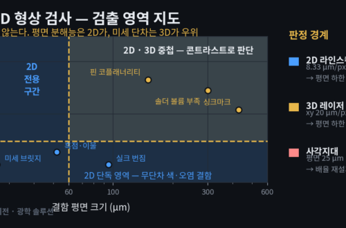
Not every inspection target needs 3D structured-light inspection. If the target component is planar and defects are mainly printing defects or foreign-matter detection that show up clearly as color/pattern differences, 2D inspection can still be favorable in terms of processing speed and equipment cost. Conversely, when the essence of a defect is a “height difference” — lifted leads, insufficient solder height, component coplanarity — 2D contrast alone has an inherent limitation, and 3D structured-light inspection is needed. However, as covered above, on material/shape combinations with very strong specular reflection, regions where the structured-light pattern itself is lost can remain, so whether actual detection is achievable in such a case cannot be confirmed before sample testing.
Field Checkpoints
- Confirm that WD (working distance) is secured with enough margin that it does not interfere with the physical placement of multi-directional projectors and camera.
- Identify in advance the reflectivity by surface material of the inspection target (specular reflection of solder vs. diffuse reflection of substrate/resist), and check whether 2D supplementary illumination or multi-directional illumination-switching logic is in place for specular regions.
- Rather than applying a single height threshold across the entire target, set coplanarity criteria separately by lead, solder, and component case.
- When introducing a new component or solder material, always re-confirm through sample testing whether structured-light pattern loss occurs.
References
- [1] 3D AOI industry trends (2026), reports of 60–80% reduction in false-call rate and roughly 30% increase in detection rate via structured-light/laser-triangulation/moiré interferometry methods
- [2] JLCPCB, “3D AOI Inspection: Why It Beats 2D AOI in PCB Assembly”
- [3] MIRTEC MV-6 OMNI 3D Inline AOI system published specifications (Blue DLP moiré, 15 MP camera, 10–15 µm telecentric lens, ±5 µm height accuracy)
- [4] Koh Young Technology, history of commercializing dual-projection-moiré-based 3D SPI in 2002 and 2026 announcement of expansion into semiconductor and advanced packaging
- [see patent] US7245387B2 (publication US20050254066A1) — CKD Corp, “Three-dimensional measuring instrument” (phase-shift 3D solder-height measurement)
- [see patent] US7400413B2 — Koh Young Technology Inc, “Three-dimensional shape measuring apparatus using shadow moire”
- [see patent] US8437533B2 — Koh Young Technology Inc, “Method of measuring a three-dimensional shape”
※ The specific figures above (defect size, accuracy, WD, etc.) are example baselines and require re-verification through sample testing before actual application.


You May Also Like
Highly Reflective Surface Defects: One Filtering Order Decides the Outcome — Bilateral Filters and the Division of Labor with Onboard AI Cameras
Where the μm Step Disappears: Measuring Both-Side Thickness Simultaneously with a Two-Channel Chromatic Confocal Controller