How Do You Inspect a Film You Cannot See? — Catching PCB Conformal Coating Gaps with UV Fluorescence Lighting and Long-Pass Filters
LIGHTING / UV FLUORESCENCE
PCB conformal coating inspection keeps stopping at the same wall. The coating film is nearly transparent in the visible band, and its surface is smooth, so specular reflection is strong. Under white illumination, the reflectance difference between coated and uncoated areas is marginal, and almost no contrast appears. This is why many processes still rely on an operator tilting the board under oblique light and checking by eye.
Left unaddressed, the cost shows up after shipment. Areas with missing coating stay exposed to moisture and ionic contamination, and thinly coated areas pass the initial inspection only to surface later as leakage current or corrosion through temperature-humidity cycles. Conversely, when coating spreads into a keep-out area such as connector contacts, contact failures follow. Because defects in both directions start from an “invisible film”, the variation in visual inspection translates directly into the field failure rate.
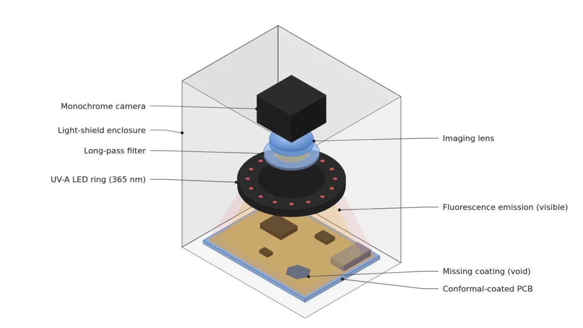
The solution is to stop trying to “see the coating through reflection” and instead capture the light the coating emits by itself. Many conformal coating materials contain a UV fluorescent tracer. When excited in the UV-A 365 nm band, the coating emits visible light at a longer wavelength, and once a long-pass (blocking) filter removes the excitation light, only the coated areas remain bright. It is a lighting design that turns a reflectance problem into an emission problem.
A transparent film cannot be seen through reflection. You have to look at the light the film emits.
1. Stokes Shift — Capturing “Emission”, Not Reflection
Point. The contrast of UV fluorescence lighting comes not from a reflectance difference but from a wavelength difference.
Reason. A fluorescent molecule absorbs a short-wavelength photon and enters an excited state, then loses part of the energy as heat and emits a photon at a longer wavelength. The gap between the absorption and emission wavelengths is called the Stokes shift. Thanks to this gap, the detection side can separate “the light that came in” from “the light the sample produced” by wavelength. In white-light inspection, the incident and reflected light share the same wavelength, so contrast flips with surface gloss and angle; in fluorescence inspection, there is simply no emission where there is no coating, so the decision axis becomes simple.
Example. Assume the coating fluoresces in the blue band when excited in the 365 nm band. The coated solder mask glows uniformly blue, while pinholes or skipped areas with missing coating remain as dark holes. A missing area a few hundred µm in diameter, barely visible under white light, becomes a clear dark blob in the fluorescence image. However, the emission band and intensity vary with the coating material and tracer concentration, so the actual emission peak must be confirmed by spectral measurement before deployment.
Point. The first line of a fluorescence inspection design is not “how many lx to illuminate with” but “how far apart the excitation band and the emission band are”. Note also that UV excitation light cannot be managed in lx, which is based on the sensitivity curve of the human eye; it must be measured and managed as irradiance in mW/cm².
2. The Long-Pass Filter Is a Precondition, Not an Option
Point. A fluorescence setup without a long-pass filter is not fluorescence inspection but UV reflection inspection.
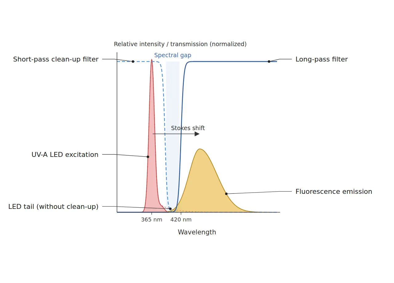
Reason. Fluorescence emission is far weaker than the excitation light. The 365 nm light reflected back from the sample surface can be several orders of magnitude stronger than the fluorescence, and silicon sensors still retain sensitivity in this band. Shoot without a filter, and specular reflections from solder fillets and metal pads dominate the frame while the fluorescence is buried beneath them. That is why a long-pass filter that blocks the excitation band and passes only the emission band is mandatory in front of the camera lens. One more thing is needed here. The emission spectrum of a UV LED is not a perfect line but has a tail toward longer wavelengths, and when this tail overlaps the passband of the long-pass filter, specular reflections from metal surfaces are captured brightly as “false fluorescence”.
Example. If solder joints appear brighter than the coated area with only the long-pass filter mounted, specular reflection of the LED tail component should be suspected first. Adding a short-pass clean-up filter in front of the LED to cut the leakage toward the emission band creates a “spectral gap” where the illumination-side and detection-side filters do not overlap. Metal surfaces mix diffuse and specular reflection, so the residual leakage cannot be confirmed before sample testing.
Point. Filter design should be thought of not as a single filter but as a pair: a short-pass on the excitation side plus a long-pass on the detection side. This gap cannot be replaced by adjusting a software threshold — the reflected light that leaked in has already been summed into the same pixel value as the fluorescence.
3. Fluorescence Intensity Is a “Thinness Alarm” — Plus Light Shielding and UV Safety
Point. Rather than trying to “measure” film thickness from fluorescence intensity, it is physically more honest to use it as an indicator that alarms on thin areas.
Reason. The fraction of excitation light absorbed by the film follows 1 − e−αd for absorption coefficient α and thickness d. In the thin range where αd is small, this value is nearly proportional to αd, so fluorescence intensity tracks thickness linearly; in the thick range it saturates, and thickness differences no longer show up as intensity differences. The interesting point is that this linear range coincides exactly with the “thinly coated areas” we need to find. Fluorescence inspection falls short as a thickness gauge but fits well as a thinness alarm.
Example. Taking the fluorescence map of a properly coated board as the reference and computing the per-pixel intensity ratio, you can design a two-stage decision: an intensity ratio below 0.3 is missing coating, and 0.3 to 0.7 is a thin area. Two conditions must come along with it. First, fluorescence is a weak signal, so unless ambient light at the sample plane is shielded down to below 1 lx, the blue component of 500 lx factory lighting passes straight through the long-pass filter and shakes the reference map. Second, UV-A carries a photobiological hazard to the eyes and skin, so the shielding cover must combine leak blocking, a door interlock, and a UV-blocking viewing window, and the light source’s risk group classification under IEC 62471 must be checked.
Point. The shielding cover is a safety device and at the same time a contrast device. The quality of the cover determines the stability of the fluorescence reference map.
In fluorescence inspection, the first optical components to design are not the lens but the filter pair and the shielding cover.
4. Core Framework — Matching Table
| Category | Item | Specification / Parameter | Basis & Notes |
|---|---|---|---|
| ① Minimum defect size | Missing coating (pinhole / skip) | Diameter 300 µm or more | Design assumption. About 6.1 px at 49 µm/px |
| ① Minimum defect size | Thinly coated area | 1 mm × 1 mm or more | Design assumption. About 20 × 20 px, subject to intensity-ratio decision |
| ① Minimum defect size | Spread into keep-out area (connector contacts, etc.) | Width 250 µm or more | Design assumption. About 5.1 px |
| ② Optical setup | Excitation lighting | UV-A 365 nm band LED ring with short-pass clean-up filter | Irradiance measured and managed in mW/cm². Purpose: block the LED long-wavelength tail |
| ② Optical setup | Detection filter | Long-pass filter, cut-on near 420 nm | Design assumption. Finalized after spectral measurement of the coating emission peak |
| ② Optical setup | Camera & lens | Mono 2448 × 2048 px (3.45 µm pixels), focal length 16 mm | Design assumption. Sensor width about 8.45 mm |
| ② Optical setup | WD (working distance) | 220 mm or more must be secured | Thin-lens object distance about 243 mm (calculated). Measure including ring light and filter holder thickness |
| ② Optical setup | FOV & pixel resolution | FOV 120 mm × 100 mm, 49 µm/px | Calculated as 120 mm ÷ 2448 px |
| ② Optical setup | Light shielding | Residual ambient light at sample plane below 1 lx | Design assumption. Based on a 500 lx factory lighting environment, with door interlock |
| ③ Algorithm | Background correction | Subtract the autofluorescence image of the uncoated board per pixel | Removes autofluorescence of solder mask and component bodies |
| ③ Algorithm | Intensity-ratio decision | Versus reference map: < 0.3 missing, 0.3 to 0.7 thin | Design assumption. Valid only within the linear range |
| ③ Algorithm | Blob filter | Report only equivalent diameter 6 px (≈ 294 µm) or more | Suppresses single-pixel noise. Consistent with 300 µm missing coating |
| ③ Algorithm | Mask | Separate coating area, keep-out area, and tall-component shadow area from design data | Shadows handled separately so they are not misjudged as missing coating |
Table implication. 120 mm ÷ 2448 px gives a pixel resolution of 49 µm/px, and 2048 px vertically × 49 µm ≈ 100 mm matches the FOV. The smallest defects, a 250 µm spread and a 300 µm missing area, occupy about 5.1 px and 6.1 px respectively, comfortably above the 3 px detection premise. Therefore, what sets the detection floor of this configuration is not pixel resolution but the leakage of the filter pair and the quality of ambient light shielding, and the right order is to confirm the spectral gap before raising the resolution.
5. When the Opposite Approach Wins
- When the coating material has no fluorescent tracer: With no emission at all, the fluorescence method does not hold. Reflection-based methods using low-angle oblique light or polarization should be considered.
- When the absolute film thickness must be guaranteed in µm: Fluorescence intensity is a relative indicator and saturates in the thick range. Interference or confocal thickness measurement methods are favorable.
- When the autofluorescence of the board or components overlaps the coating emission band: Contrast stays low even after background subtraction. Changing the excitation wavelength or a visible-light-based method may be more economical.
The emission spectrum of the coating material, board autofluorescence, and diffuse-reflection leakage from solder and metal surfaces depend heavily on material lots and process conditions, so the outcome cannot be confirmed before sample testing.
Field Note
While setting up a coating inspection station on a high-speed assembly line, I once looked at the first image with only a long-pass filter mounted and found the solder fillets glowing brighter than the coated area, which flipped the decisions. Raising the filter cut-on did not solve it because the fluorescence dropped along with it; the false fluorescence disappeared only after I added a short-pass clean-up filter in front of the LED. Later I also ran into the reference map drifting at every shift change because of ceiling light leaking through gaps in the shielding cover. Only after bringing the residual illuminance at the sample plane below 1 lx did the 0.3 to 0.7 intensity-ratio decision stabilize, and it is quite likely that this boundary will need to be set again whenever the material changes.
Field Checkpoints
- Is a WD of 220 mm or more secured by actual measurement? — Check including the UV ring light housing, filter holder, and shielding cover thickness.
- Have you first identified the target surface material and reflectance? — Leakage risk varies with the specular share of the solder mask, solder fillets, and metal pads.
- Have you confirmed by spectral measurement whether the coating material has a fluorescent tracer and where its emission peak is?
- Is there a spectral gap between the LED emission tail and the long-pass filter passband? — If not, add a short-pass clean-up filter.
- Is the residual ambient light at the sample plane below 1 lx both with the door open and closed?
- Are UV leak blocking, a door interlock, and a UV-blocking viewing window in place, and has the light source’s IEC 62471 risk group been checked?

Noctvision
A machine vision engineer who fits cameras, lenses, lighting, and image-processing algorithms together for a living. Years spent on continuous production lines, vibration, heat, and dust included, working through diffuse reflection, contrast, and resolution differences too fine for a spec sheet to capture inform every post here, closing the gap between theory and the shop floor. Off duty, that same eye for light and lenses goes into repairing fully mechanical vintage film cameras.


You May Also Like
Why Does One Lighting Angle Decide OCR Read Rates on Molded Characters? — Low-Angle Ring Illumination and Quadrant Lighting Calculated from Character Height and Stroke Spacing
How to Handle Imaging on Highly Reflective Surfaces