Can’t You Catch Color Differences Without a Color Camera? — Building PCB Solder Mask, Silkscreen and Copper Pad Contrast with a Mono Camera and Wavelength Selection
LIGHTING / OPTICS
The most common request in PCB visual inspection is “the colors are different, so let’s look with a color camera”. Green solder mask, white silkscreen print and reddish-brown copper pads are clearly different colors to the human eye, so it seems a color image would separate them easily. Yet when actually imaged with white illumination and a color camera, a thin silkscreen smear on the mask or copper exposed through a gap where the mask has lifted often does not separate as sharply as expected.
Left unaddressed, the cost appears at the small defects on the borderline. Lowering the threshold while contrast is insufficient floods the line with over-detections from gloss mottling of the mask and print density differences, and raising the threshold lets an 80 µm-class mask peel pass. When the resolution loss of a color camera is added on top, the smallest defects are scattered over just a few pixels from the start, and the judgment itself becomes unstable. In the end, a re-inspection step where an operator looks again by eye remains.
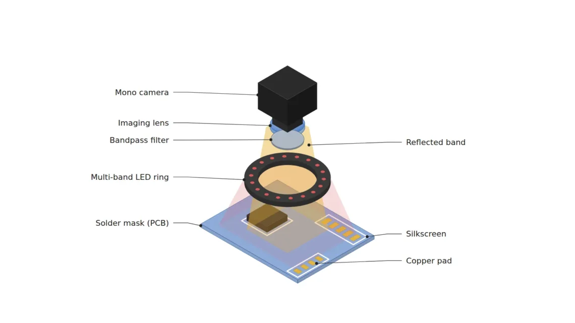
The solution is not to “capture” color but to choose the wavelength and create contrast at the illumination stage. Combining a mono camera with narrow-band color LEDs lets you illuminate with only the wavelength where the band-by-band reflectance difference between two materials is largest. Applying the simple principle that complementary-color illumination darkens a target and same-color illumination brightens it to the three materials of a PCB yields both higher resolution and greater contrast than a color camera.
What a mono camera sees is not color but the reflectance difference at the chosen wavelength.
1. Complementary Darkens, Same Color Brightens — The Principle of Band Selection
Point. The criterion for choosing color LED illumination is not “what color is the target” but “at which wavelength is the reflectance difference between the two materials largest”.
Reason. The color of an object is the shape of its reflectance curve over wavelength. Solder mask that looks green returns relatively more of the green band and absorbs the red and blue bands. Therefore, under red illumination (the complementary side) the mask images dark, and under green illumination (the same color) it images relatively bright. A mono sensor records only the amount of light that comes in, so changing the illumination wavelength is the same as changing the brightness order of the materials. Contrast is decided not by the sensor but by how the illumination spectrum and the reflectance curves overlap.
Example. Copper is a material whose reflectance is low on the short-wavelength side and rises toward longer wavelengths, which is why it looks reddish-brown. White silkscreen reflects the whole visible band relatively evenly. Overlaying these three curves, at red 625 nm copper and silkscreen are bright and the mask is dark; at blue 470 nm silkscreen is bright and copper becomes relatively dark; and at green 525 nm the mask brightens, reducing the contrast between the mask and the other materials. The actual values of each curve vary with the mask formulation and the copper surface finish, so the brightness in each band must be measured.
Point. Decide band selection by the difference between curves, not by experience. The fact that the band with the largest reflectance difference is different for each material pair to be detected is the starting point of this design.
2. How to Assign Bands to the Three PCB Materials
Point. In PCB inspection, rather than trying to catch every defect with one band, it is more accurate to assign separately, for each defect type, the band where contrast is maximal.
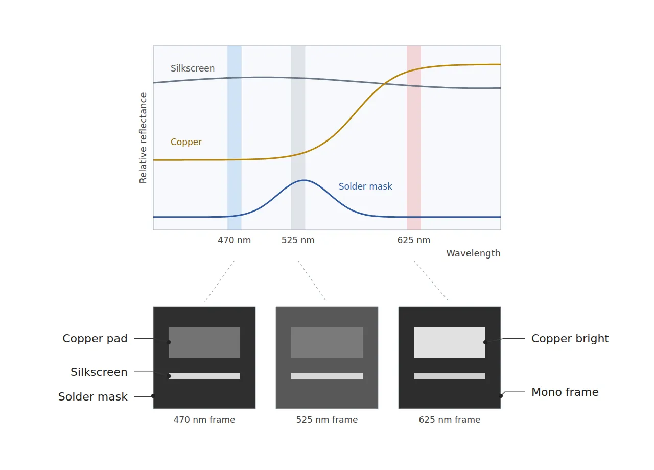
Reason. Finding copper exposed by mask peeling is a “copper vs. mask” contrast problem, and finding silkscreen smeared onto a pad is a “silkscreen vs. copper” contrast problem. The wavelengths at which the reflectance difference of the two pairs is maximal differ from each other. Trying to solve both problems at once with one band sacrifices the contrast of one pair, and that sacrifice ends up being filled by threshold adjustment. Software image processing alone cannot fully restore contrast that the illumination did not create.
Example. The red 625 nm frame is assigned to detecting copper exposure (mask peel) and missing pad areas. Copper is bright and the mask is dark, so the boundary is sharp. The blue 470 nm frame is assigned to detecting silkscreen smear on pads, because the silkscreen is bright and copper becomes relatively dark. The green 525 nm frame uses the same-color principle to brighten the mask background and is used to highlight dark foreign particles or scratches on the mask. Lighting the three bands sequentially and taking three images secures the one image most favorable for each defect type. However, glossy mask is a diffusely reflecting material in which specular reflection mixes in depending on the illumination angle, so, including the possibility that the per-band contrast order changes, this cannot be confirmed before sample testing.
Point. Make the band assignment table first, and then design the algorithm separately for each band. The illumination creates the contrast, and the algorithm should take on only the role of reading that contrast.
If there are two material pairs to detect, there are also two optimal bands. A single white-light image cannot capture both pairs at maximum contrast.
3. Pros and Cons Compared with White Light + Color Camera
Point. For the same sensor size, a mono camera + wavelength-selective illumination is favorable in resolution and contrast, while white light + a color camera is favorable in single-shot capture and versatility.
Reason. A typical color sensor places only one of the R, G or B filters on each pixel in a Bayer pattern. Red and blue pixels occur once every 2 px horizontally and vertically, so looking at the red channel alone, the sampling interval is twice that of mono. Demosaic interpolation only fills in the empty pixels and does not restore real resolution. Also, the passbands of color filters are broad and overlap each other, so the separation between channels is duller than the reflectance difference created by narrow-band LEDs. On the other hand, a color camera obtains three channels simultaneously in one shot, so it is strong with moving targets and unknown discoloration defects.
Example. Viewing a 40 mm FOV with a 2448 × 2048 px sensor gives a mono pixel resolution of about 16.3 µm/px, and an 80 µm mask peel occupies about 4.9 px. In the color version of the same sensor, the sampling interval of the red channel is about 32.7 µm, so the same defect shrinks to about 2.4 samples, falling below the 3 px detection premise. The price of mono sequential capture is three images, and the bands must be switched while the target is stationary. In addition, the quantum efficiency of a mono sensor differs by wavelength, so the exposure of each band must be normalized with a white reference plate for the brightness scales of the three images to match.
Point. Before choosing a color camera, first calculate how many samples the minimum defect occupies at the color channel sampling interval. If it falls short of 3 samples, resolution runs out before color information does.
4. Core Framework — Matching Table
| Category | Item | Specification / Parameter | Basis & Notes |
|---|---|---|---|
| ① Minimum defect size | Solder mask peel (copper exposed) | 80 µm or more | Design assumption. Occupies about 4.9 px at 16.3 µm/px |
| ① Minimum defect size | Silkscreen smear on pad | 100 µm or more | Design assumption. Occupies about 6.1 px |
| ① Minimum defect size | Pad discoloration / contamination | 150 µm or more | Design assumption. Occupies about 9.2 px |
| ② Optical setup | Illumination | Multi-channel ring light (470 / 525 / 625 nm), with diffuser, sequential lighting | Design assumption. Per-band contrast finalized by measurement |
| ② Optical setup | Band assignment | 625 nm: copper exposure & missing pad / 470 nm: silkscreen smear / 525 nm: foreign particles on mask | Initial assignment based on the complementary / same-color principle |
| ② Optical setup | Lens | Focal length 25 mm, F/5.6 | Magnification about 0.211×, calculated object distance about 143 mm |
| ② Optical setup | WD (working distance) | 120 mm or more must be secured | Measured from the lens front end. Verify by measurement including ring light height and component height |
| ② Optical setup | Sensor & FOV | Mono 2448 × 2048 px, 3.45 µm pixels / FOV 40 mm × 33.5 mm | 40 ÷ 2448 ≈ 16.3 µm/px (calculated value). Color R channel at about 32.7 µm interval |
| ③ Algorithm | Band normalization | Per-band exposure correction with a white reference plate, equalizing reference brightness | Corrects quantum efficiency differences by wavelength |
| ③ Algorithm | Contrast metric | Michelson contrast per material pair (Imax − Imin) ÷ (Imax + Imin) ≥ 0.3 | Design target. Reassign bands if not met |
| ③ Algorithm | Band ratio image | Pixel-wise 625 nm ÷ 470 nm ratio to separate copper regions | Less sensitive to illumination brightness variation |
| ③ Algorithm | Defect judgment | Per-band region difference > 3σ, minimum area 12 px or more | Based on an 80 µm defect area of about 4.9 × 4.9 px = about 24 px |
Table implication. At mono 16.3 µm/px, the minimum defect of 80 µm is about 4.9 px, comfortably exceeding the 3 px detection premise. With the color version of the same sensor, it would be only about 2.4 samples on the red channel basis, so the detection premise collapses in exactly the channel that best reveals copper exposure. The reason to choose mono + band selection at the takt cost of three images lies not in color discrimination but in this resolution difference.
5. When the Opposite Approach Wins
- When the color of the defect is not determined in advance: If color itself is the judgment criterion, as in discoloration grading or unknown contamination, white light + a color camera that obtains three channels at once is favorable.
- When the target is moving and sequential capture is difficult: The position shifts while three images are taken with switched bands, so a color camera capable of single-shot capture is favorable in both takt and registration.
- High-mix lines where the mask color changes frequently by model: The complementary band differs for blue, black and red masks, so if the burden of managing a band assignment table per model is large, a color camera is operationally simpler.
The per-band reflectance difference varies greatly with solder mask gloss and copper surface finish, so which approach has the advantage cannot be confirmed before sample testing.
Field Note
I once started PCB visual inspection on a high-speed assembly line with a color camera and changed the configuration because small mask peels were smeared out in the red channel. I attached a 470 / 525 / 625 nm ring light to a mono camera and first matched the per-band exposure with a white reference plate, and the boundary of copper exposure became distinctly sharper in the 625 nm frame. However, on a mask model with strong gloss, specular reflection from the ring light mixed in and the contrast of the 470 nm frame was lower than expected, and only after adding a diffuser did the Michelson contrast exceed 0.3. Even with the same green mask, the curve can change when the supplier changes, so even now I measure the per-band contrast first for every new model.
Field Checkpoints
- Is a WD of 120 mm or more secured by actual measurement? — Measure from the lens front end, including the ring light height and the height of mounted components.
- Have the color and gloss of the solder mask and the copper surface finish been checked first? — If the reflectance curve changes, the band assignment changes too.
- Has the per-band Michelson contrast been measured for each material pair to be detected, and an assignment table made?
- If a color camera is under consideration, does the minimum defect span 3 samples or more at the channel sampling interval?
- Has the per-band exposure been normalized with a white reference plate? — Sensor quantum efficiency differs by wavelength.
- Does the target stay stationary during the three sequential captures, and does it fit within the takt?

Noctvision
A machine vision engineer who fits cameras, lenses, lighting, and image-processing algorithms together for a living. Years spent on continuous production lines, vibration, heat, and dust included, working through diffuse reflection, contrast, and resolution differences too fine for a spec sheet to capture inform every post here, closing the gap between theory and the shop floor. Off duty, that same eye for light and lenses goes into repairing fully mechanical vintage film cameras.


You May Also Like
2D/3D Fusion Inspection: The Bottleneck Is Lighting Interference
There Are Defects That Vanish in Visible Light — Inspection Design Beyond the 1 μm Barrier in SWIR Imaging