Few-Shot Anomaly Detection: Can 5 Defect Samples Stand Up an Inspection Line
There’s a question that repeats every time a new line is set up. “How many defect samples do we need to collect before we can run an inspection model?” Whether it’s an injection-molded part or a PCB, early in mass production you can secure thousands of normal-part images, but defective ones are few and far between. Leaving this imbalance unaddressed causes the inspection line to break down in two ways. First, if you force-lump defect types into a handful of classes and train on that, both over-detection and missed detection spike every time a new defect pattern appears. Second, if you substitute manual visual inspection until enough data accumulates, the leakage cost during that period flows straight into downstream processes and customer claims. A recently emerging approach to this dilemma is few-shot anomaly detection — a method that establishes a detection boundary using mostly normal-sample data plus only a handful (5–20) of defect samples.
What is few-shot anomaly detection
Point: Few-shot anomaly detection takes the “feature space of normal data” as its reference, and judges any point that deviates from that boundary as an anomaly.
Reason: Defect types — micro-cracks, scratches, foreign matter, discoloration on an injection-molded part — form a combination space that is effectively infinite, while normal patterns are comparatively homogeneous. That’s why measuring “how far a sample has drifted from normal” is far more data-efficient than trying to “classify defects.”
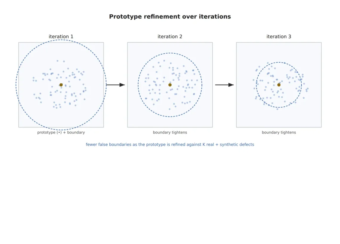
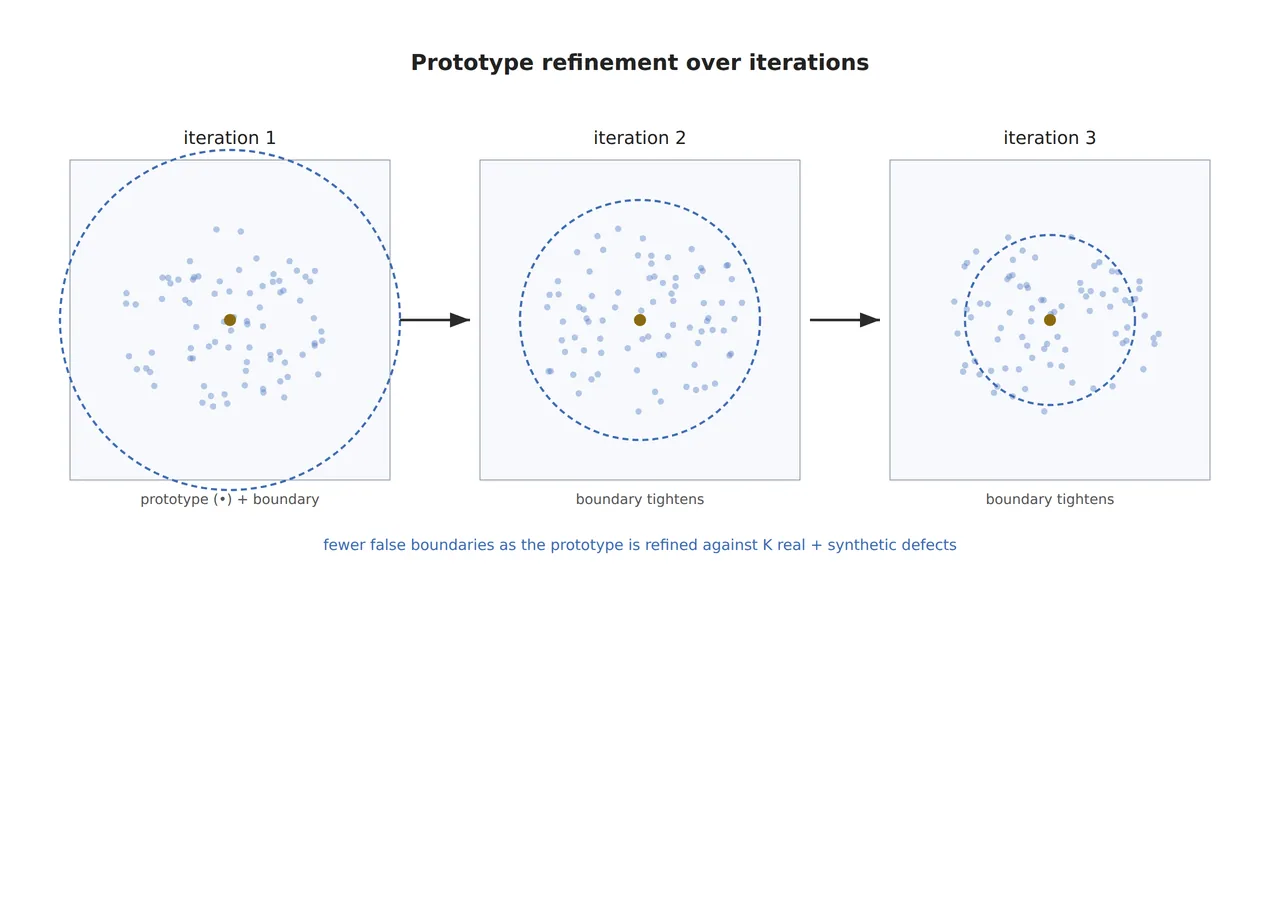
Example: FastRef, presented at CVPR 2026, proposed a framework that iteratively refines prototypes — a small number of reference points representing normal features — to narrow the gap between the prototypes and the actual feature distribution using only an extremely small number of samples. Around the same time, the Calibrated Feature Fusion study addressed a method for aligning (calibrating) features extracted from multiple layers of a Vision Transformer (ViT) to stably localize micro-defects even from a small sample set.
Point: Ultimately, the core of few-shot anomaly detection comes down to “how few prototypes, drawn how accurately, can trace the boundary of normal.”
Prototype refinement and synthetic anomaly generation
Point: Because prototype refinement alone is vulnerable to noise early in training, a parallel trend has taken hold: combining it with synthetic anomaly generation.
Reason: Even with only 5 real defect samples, transforming the features of that small sample set with a diffusion model or feature-manipulation techniques to mass-produce fake defects for training secures the contrastive data needed for the prototype-refinement stage.
Example: In semiconductor wafer inspection, this exact structure already exists as an issued patent. KLA Corporation’s US Patent US10599951B2 (“Training a neural network for defect detection in low resolution images”) claims a structure in which a high-resolution imaging subsystem and a neural network synthetically generate defect images, and this synthetic data is used to train a neural network for low-resolution inspection. In that it enables high-speed inspection without a large volume of real, low-resolution defect data, the problem framing overlaps precisely with few-shot anomaly detection on PCB and injection-molded-part lines.
Point: In other words, the structure of “defects synthesized at high resolution → a real-world model trained at low resolution” is a validated approach applicable well beyond semiconductors, across high-mix, low-volume production lines in general.
Core framework matching table — detection size, optical setup, algorithm parameters
The table below is organized around two representative cases: PCB micro-cracks and injection-molded surface defects. In an actual project, the target’s surface material and reflectivity should be confirmed first, before adjusting the lighting and lens specifications.
| Category | ① Minimum detectable defect size | ② Optical setup | ③ Algorithm parameters |
|---|---|---|---|
| PCB micro-crack | 30 µm | Coaxial epi-illumination + telecentric lens, WD 90 mm secured, magnification 1×, defect corresponds to 8–9 px at a 3.45 µm pixel size | Few-shot K=10, ViT-B/16 backbone, 3 prototype-refinement iterations, anomaly-score threshold top 2σ |
| Injection-molded surface scratch/foreign matter | 50 µm | Low-angle dark-field illumination + macro lens, WD 120 mm secured, illuminance 8,000 lx | Few-shot K=20, ResNet-50 backbone, synthetic-to-real defect ratio 8:1, anomaly-score threshold top 2.5σ |
Takeaway: In both cases, real defect samples are kept to roughly 10–20, while the structure first maximizes defect contrast at the optical-setup level, then absorbs the remaining variability through the algorithm’s prototype count and synthetic ratio. Unless lighting and lens choices secure the signal-to-noise ratio first, no amount of prototype refinement will keep the feature space itself from blurring — and the advantage of few-shot anomaly detection disappears with it.
The data infrastructure is evolving too
Point: For few-shot anomaly detection to take hold on the floor, the camera/sensor-side data infrastructure has to support it as well.
Reason: Even a small sample set has to be captured at high resolution and high speed without dropped frames, or the input quality feeding prototype refinement is not guaranteed.
Example: In May 2026, A3 (the Association for Advancing Automation) officially released GigE Vision 3.0, which introduces the GigE Vision RDMA Streaming Protocol (GVRSP) built on RoCEv2 (RDMA over Converged Ethernet v2), transferring data directly from the camera to host memory to reduce CPU load and latency. The same year, Sony successively announced the IMX947, a roughly 26MP/383fps global-shutter industrial sensor, and the IMX711, an X-ray CMOS sensor built for low-noise, high-speed imaging. These interface and sensor advances form the hardware foundation for pulling the “small but clean data” that few-shot anomaly detection requires, in real time, at line speed.
Point: No matter how data-efficient an algorithm is, guaranteeing the signal quality of that small sample set ultimately falls to the optical and interface layers.
A comparative note — few-shot isn’t always favorable
On a line where the normal pattern itself is highly variable and process deviation is large — for example, a material whose surface texture swings significantly lot to lot — the prototypes in few-shot anomaly detection risk mistaking normal variation for a defect. In such cases, feeding more labeled data into a traditional supervised classification model can be the more stable choice. However, this depends on the variability specific to the material and process, so it cannot be confirmed before sample testing.
Field Checkpoints
- Has it been confirmed that the camera/lens WD (working distance) is actually achievable at the target magnification?
- Has it been pre-checked, for both normal samples and the small set of defect samples, that the defect contrast under the optical setup is distinguishable even to the naked eye?
- Has the synthetic-to-real defect generation ratio been reviewed to confirm it does not distort the line’s actual defect-type distribution?
- Have the number of prototype-refinement iterations and the anomaly-score threshold been re-verified against a separate validation set?
- Has it been confirmed that the data-transfer interface (GigE, etc.) has enough bandwidth to acquire images without a bottleneck within the inspection cycle time?
References
- A3 (Association for Advancing Automation), “A3 Officially Releases GigE Vision 3.0, Opening New Possibilities in Machine Vision” (2026-05-12)
- Sony Semiconductor Solutions, IMX947 global-shutter sensor and IMX711 X-ray CMOS sensor news releases (2026)
- FastRef: Fast Prototype Refinement for Few-Shot Industrial Anomaly Detection, CVPR 2026
- Calibrated Feature Fusion: Enhancing Few-Shot Industrial Anomaly Detection via Cross-Stage Representation Alignment (2026)
- US10599951B2, “Training a neural network for defect detection in low resolution images”, KLA-Tencor Corporation
- US8614415B2, “Defect inspection method of fine structure object and defect inspection apparatus”, NEC Corporation


You May Also Like
What You Must Check Before Applying INT8 Quantization to Edge AI Inference: Why Micro-Defects Quietly Disappear
AOI Only Says “Defective” — How Vision Language Models Fill the Gap in Judgment Rationale