Changing the Sensor Means Recalculating the Illumination — What 15% Quantum Efficiency at 940 nm on a BSI Global Shutter Sensor Actually Means
OPTICS / LIGHTING
The reason for moving to near-infrared (NIR) illumination is usually clear. Under visible light the color of printing, paint, and labels dominates the background contrast and buries defects, but near 940 nm the absorption of many organic dyes drops sharply, so the color disappears and only the structure remains. Fine cracks in a connector housing, foreign inclusions in a molded part, and unfilled regions in an adhesive layer suddenly become visible at this point.
Yet a great many lines that switch to NIR on the shop floor run into the same problem. They leave the illumination as it is and change only the wavelength, and the image is dark; they lengthen the exposure, and motion blur appears on targets in motion; they raise the gain, and noise buries the defect signal. Left unaddressed, the outcome converges in one direction — loosening the detection threshold and creating escapes, or tightening it and causing false calls to explode. Either way it is a failure against a standard of 0% false calls and 0% escapes.
The cause is usually not the sensor selection but the failure to recalculate the illumination budget. The published quantum efficiency (QE) of the new BSI global shutter sensor announced on 22 September 2026 makes this calculation very concrete.
The decision to change wavelength does not end in the sensor catalog; it ends in the illumination power supply capacity table.
1. Check the Surface Material and Reflectance First
Point. Before reviewing a BSI global shutter sensor, you must first check how the target surface reflects at 940 nm.
Reason. The reason useful contrast appears in the near infrared is not the sensor but the difference in spectral reflectance between materials. It is common for two regions that looked like different colors under visible light to converge to the same reflectance in the near infrared, so that contrast actually disappears. Conversely, a material boundary that was indistinguishable under visible light may be revealed in the near infrared. Which of the two occurs depends on the material and the surface treatment, so it cannot be determined from catalog specifications alone.
Example. If the black pigment is a carbon black type, it still absorbs strongly in the near infrared and remains dark, but if it is an organic black dye type, transmission rises in the near infrared and the structure underneath shows through. The very same “black plastic connector” produces opposite images depending on the pigment type.
Point. In other words, the first step of an NIR transition is not sensor selection but verifying 940 nm reflection and transmission on real samples. Especially for machined surfaces with heavy diffuse reflection, or lots with large variation in surface treatment, this cannot be guaranteed before a sample test.
2. What BSI Actually Changes — The Path the Photon Travels
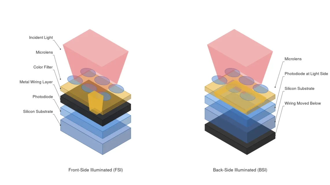
Point. The benefit of the BSI (backside illuminated) structure is not the vague statement that “sensitivity improves”, but the structural fact that photons no longer pass through the wiring layer.
Reason. In the traditional FSI (front-side illuminated) structure, incident light reaches the photodiode by passing between metal wiring layers. As the pixel shrinks, the fraction occupied by wiring grows, the effective aperture (fill factor) decreases, and obliquely incident rays are blocked by the wiring or leak into neighboring pixels, creating crosstalk. BSI flips the wafer and places the photodiode on the incident side, so this path loss disappears structurally.
Example. The Nexora family announced by Teledyne e2v on 22 September 2026 is a global shutter CMOS sensor family for machine vision that adopts this structure. The published specifications are 12 MP (4,096 × 3,072) and 16 MP (4,096 × 4,096), monochrome and color versions, and QE of up to 73% at 550 nm and 15% at 940 nm. It also applies a 3D-stacked structure, the package is 23 × 21.5 mm and is compatible with 29 × 29 mm² cameras and standard C-mount optics, and the interface is LVDS. Documentation and samples were stated to be available upon request at the time of announcement.
Point. The number to watch here is not 73% but 15%. Even after the improvement from BSI, silicon remains weak at 940 nm, and the fact that the degree of that weakness is now given quantitatively is far more useful to a designer.
3. The Illumination Budget — Read the QE Ratio Directly as a Multiplier
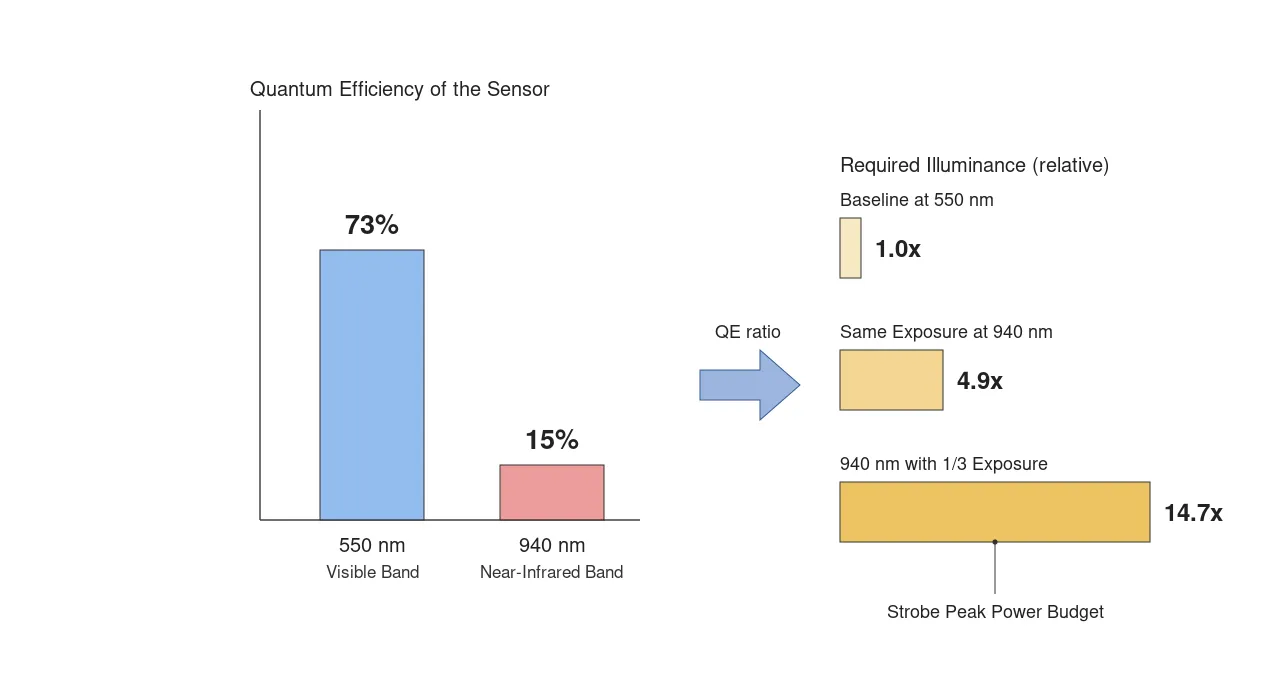
Point. With the same sensor, the same lens, and the same exposure time, changing 550 nm illumination to 940 nm raises the required irradiance by exactly the QE ratio in order to obtain the same number of signal electrons.
Reason. The number of signal electrons generated at the photoelectric conversion stage is the product of the incident photon count and the QE. Holding everything else fixed, when the QE falls from 73% to 15%, the required photon count becomes 73 ÷ 15 ≈ 4.9 times. This is not an estimate but the arithmetic ratio of the two published QE values, and it is a lower bound that does not yet include lens transmission, target reflectance, or bandpass filter losses. In a real design, optical losses multiply on top of this.
Example. Suppose you also apply a design that cuts the exposure to 1/3 in order to suppress motion blur during inspection in motion. The required illuminance multiplier then becomes 4.9 × 3 ≈ 14.7 times. Continuous illumination cannot absorb this multiplier without exceeding heat and power supply limits, so in practice the design usually moves to strobe (pulsed) illumination, lowering the duty cycle and raising the peak current. A global shutter is a precondition for that move — with a rolling shutter, a short strobe pulse lands on only some rows and creates banding.
Point. The core insight of this article is this. The NIR QE figure of a sensor is not a sensor specification but an illumination power specification. The “15%” in the catalog should be read by the illumination designer as the instruction “budget roughly five times the peak power”, and only by also reading that the exposure reduction factor multiplies on top of it does the actual BOM come out right.
QE of 15% is not a weakness of the sensor; it is a coefficient that belongs in the illumination budget table.
4. Constraints Left by the Package and the Mount — Check WD First
Point. The sensor package dimensions and the mount standard define the lens selection range, and the lens selection range defines the range of working distance (WD) that can be secured.
Reason. Standard C-mount compatibility means you can use the off-the-shelf lens families built to the 17.526 mm flange back focal distance standard. Having a wide selection is an advantage, but at the same time the combinations that cover a large sensor diagonal while simultaneously satisfying the required magnification and WD narrow faster than expected. In the near infrared in particular, a lens whose chromatic aberration correction was performed only for visible light shifts its focal plane, so focus set under visible light drifts at 940 nm.
Example. A 16 MP square format (4,096 × 4,096) demands a more uniform image circle than a 4:3 format with the same pixel count. Add a multi-direction strobe illumination head occupying the area around the optical axis, and the WD must be budgeted generously from the start in order to avoid interference between the light ring and the target.
Point. In short, replacing the sensor often entails replacing the optics, and that judgment turns on whether the WD is secured by actual measurement. It must be confirmed by measurement including the illumination housing and fixtures, not by a calculated value on a drawing.
5. Core Framework — Matching Table
| Category | Item | Specification / Parameter | Basis and Notes |
|---|---|---|---|
| ① Minimum Defect Size | Fine crack in connector housing | Width 30 µm, length 300 µm or more | Design assumption. Detected by near-infrared transmission contrast |
| ① Minimum Defect Size | Foreign inclusion inside molded part | Largest dimension 80 µm or more | Design assumption. Based on transmitted illumination |
| ① Minimum Defect Size | Unfilled region in adhesive layer | Area 0.2 mm² or more | Design assumption. Targets low-frequency brightness deviation |
| ② Optical Setup | Illumination wavelength | 940 nm near infrared, bandwidth ±25 nm | The point of the published sensor QE of 15% |
| ② Optical Setup | Illumination method | Strobe (pulsed) drive, synchronized to the global shutter | Continuous illumination cannot absorb the required multiplier |
| ② Optical Setup | Illuminance multiplier (lower bound) | About 4.9 times relative to 550 nm | Arithmetic ratio of published QE 73% ÷ 15%. Optical losses not included |
| ② Optical Setup | When exposure is also shortened | About 14.7 times at 1/3 exposure | The above multiplier × the exposure reduction factor |
| ② Optical Setup | Sensor | BSI global shutter, 12 MP or 16 MP | Published specification 4,096 × 3,072 / 4,096 × 4,096 |
| ② Optical Setup | Mount and package | Standard C-mount, package 23 × 21.5 mm | Published specification. Compatible with 29 × 29 mm² cameras |
| ② Optical Setup | WD (working distance) | 180 mm or more must be secured by measurement | Measured including interference from the strobe illumination head and fixtures |
| ② Optical Setup | Lens | NIR corrected lens is mandatory | A visible-only lens shifts its focal plane at 940 nm |
| ③ Algorithm | Noise handling | Raise illuminance before raising gain | Gain does not improve SNR |
| ③ Algorithm | Flat fielding | Flat field for correcting strobe illuminance non-uniformity | Acquired separately at 940 nm |
| ③ Algorithm | Detection threshold | 3σ based on 30 good parts | σ must be re-estimated when the wavelength changes |
What the table implies. The rows that actually govern the design are the two “illuminance multiplier” lines. The sensor, lens, and algorithm rows are matters of choice, but the lower bound of 4.9 times comes from physics and is not negotiable. The correct order is for the illumination power supply capacity and thermal design to be settled first, with everything else fitted inside them.
6. Related Patents (Verified as Existing)
| Patent Number | Title | Assignee | Filing / Grant |
|---|---|---|---|
| US 9,991,309 B1 | CMOS image sensor having enhanced near infrared quantum efficiency | OmniVision Technologies, Inc. | Priority 2017-07-05 / Active |
| US 10,224,364 B2 | CMOS image sensor having enhanced near infrared quantum efficiency and modulation transfer function | OmniVision Technologies, Inc. | Priority 2017-07-05 / Published 2019-03-05 |
| US 10,964,744 B1 | Light control for improved near infrared sensitivity and channel separation | OmniVision Technologies, Inc. | Priority 2019-09-13 / Published 2021-03-30 |
| US 10,798,323 B2 | Control method for an active pixel image sensor | Teledyne e2v Semiconductors SAS | Filed 2017-01-13 / Granted 2020-10-06 |
| US 10,587,830 B2 | Method for controlling an active pixel image sensor | Teledyne e2v Semiconductors SAS | Filed 2016-07-29 / Granted 2020-03-10 |
Patents whose assignee could not be explicitly confirmed were excluded from the citation list. The last two are control methods covering the memory node and correlated double sampling (CDS) in global shutter mode, and they bear directly on the strobe synchronization design in section 3.
7. Conditions Where the Opposite Approach Is Better
- When visible light already yields sufficient contrast: An NIR transition only increases the illumination budget by about five times. There is no reason to change the wavelength.
- When the target is stationary and the tact time has margin: A long exposure is available, so the advantage of combining a global shutter with strobing shrinks. A rolling shutter with continuous illumination is more economical.
- When absorption characteristics beyond 1,000 nm must be observed: This is outside the sensitivity limit of a silicon sensor. InGaAs-based SWIR imaging is the physically correct choice.
- When individual photon-level signals must be counted at extremely low light: This is not a region solved by improving QE. Photon-counting sensors are the appropriate choice.
Even at the same wavelength, near-infrared reflection and transmission vary with the pigment type, the surface treatment, and lot variation, so this cannot be guaranteed before a sample test.
Field Note
The sequence I went through when converting a connector housing line to 940 nm was largely the same each time. First leave the illumination as it is and change only the wavelength, then lengthen the exposure because it is dark, then shorten it again because blur appears in the moving section, and only then come back to the illuminance calculation. The only way I found to skip that round trip in one step was to read the value at the target wavelength off the QE curve in the sensor datasheet first, and write that ratio at the top of the illumination specification sheet. That said, on a continuously running strip line where the target never stops, the strobe pulse width and the allowable displacement become entangled again, so this coefficient alone does not close the design. That is especially true for molded parts whose pigment type changes from lot to lot, and in the end I keep the qualifier cannot be guaranteed before a sample test attached.
Field Checkpoints
- Is a WD of 180 mm or more secured by actual measurement — verify with the strobe illumination head housing and the fixtures included.
- Has 940 nm reflection and transmission of the target surface been verified on real samples — the result comes out opposite depending on the pigment type.
- Has the illuminance multiplier been derived backward from the QE ratio — about 4.9 times from the published QE alone, and more once exposure reduction is added.
- Is the lens an NIR corrected specification — a visible-only lens shifts its focal plane at 940 nm.
- Is the shutter a global shutter — with a rolling shutter, a short strobe pulse creates banding.
- Has σ for good parts been re-estimated after the wavelength change — reusing a visible-light threshold increases both false calls and escapes at the same time.
- Are the illumination power supply capacity and thermal design based on peak power — budgeting on average power falls short under pulsed drive.
Related Developments (2026-09-16 to 09-23)
- Teledyne e2v announced the Nexora family of BSI global shutter CMOS image sensors (2026-09-22, Seville, Spain). 12 MP and 16 MP, monochrome and color, QE 73% at 550 nm / 15% at 940 nm, 3D-stacked structure, LVDS interface, package 23 × 21.5 mm, standard C-mount compatible. To be exhibited at VISION 2026 (Stuttgart, 6–8 October) Hall 8, Booth 8B10.
- Teledyne Adimec and Teledyne DALSA announced a Sony IMX927-based 100 Gbit/s imaging platform (2026-09-17, Eindhoven, Netherlands). The S-105A110 camera (105 MP, 110 fps, CoaXPress over Fiber) with the Xtium3-QSFP28 frame grabber (dual QSFP28, PCIe Gen 4). Prototype units for evaluation are expected in Q1 2027.
- LYNRED announced the CAPT640 thermal imaging sensor (2026-09-21, Grenoble, France), unveiled at AutoSens Barcelona (22–24 September).
- Excelitas announced demonstrations of optical inspection lenses and scientific cameras at VISION 2026 (2026-09-22), including a demonstration capturing at over 2,000 fps with the LINOS d.fine HR-M lens and the pco.dimax 3.6 ST high-speed camera.
- Tucsen introduced the XT Series beam quality analyzer, the Libra 27105 and Libra 5505 high-throughput cameras, and the Aries 6504 single-photon-level high-speed series at CIOE 2026 (September 2026).
- Specim (a Konica Minolta company) announced that a new hyperspectral camera will be unveiled at the start of VISION 2026.
- Edmund Optics expanded its product portfolio with a point source microscope for precision optical alignment.

Noctvision
A machine vision engineer who fits cameras, lenses, lighting, and image-processing algorithms together for a living. Years spent on continuous production lines, vibration, heat, and dust included, working through diffuse reflection, contrast, and resolution differences too fine for a spec sheet to capture inform every post here, closing the gap between theory and the shop floor. Off duty, that same eye for light and lenses goes into repairing fully mechanical vintage film cameras.


You May Also Like
How Do You Inspect a Film You Cannot See? — Catching PCB Conformal Coating Gaps with UV Fluorescence Lighting and Long-Pass Filters
The Surface You Could Only See at a Standstill — How Color-Multiplexed Strobing Breaks the Standstill Condition of Photometric Stereo