In SWIR Imaging, Lighting and Aperture Keep the Defect Contrast
OPTICS
Move the wavelength past 1.1 μm, where silicon stops, and defects hidden in visible light come out, but keeping that contrast falls to the lighting nonuniformity and the aperture.
Taking a clear molded cover with a printed film as the example, I calculated how strongly film lifting, moisture and particles each show up in SWIR imaging.
About 18 min read
1,107 nm is the longest wavelength a silicon pixel can turn into an electrical signal. It is the bandgap1 of silicon, 1.12 eV, converted to a wavelength, so a visible-light camera runs out of sensitivity around here and sees nothing at all beyond it. The 1 μm barrier in the title refers to this boundary. Beyond it, in the short-wave infrared (SWIR)2 band of roughly 0.9 to 1.7 μm, the same materials show a different face from the one they show in visible light, and defects with no contrast on a visible-light image can come out.
The inspection target is a clear PC cover made by placing a printed film inside the mold and molding resin behind it, a film insert molding3 part. With a refractive index of 1.5 assumed for both cover and film, about 4 % reflects at each surface, and the visible image is covered by the printed pattern on the film. Underneath, places where the film has lifted, moisture left after cleaning and 100 μm particles in the resin all blend into the print and vanish. If such a defect shows up after assembly, the whole cover has to be replaced, by which point the cost of other parts has already piled on.
Changing the wavelength brings contrast back, but how many percent comes back is set by the physics of the material and the defect. What I want to work out on this cover is how many percent lifting, moisture and particles each show in SWIR, and how well the pixels, the lighting and the lens protect those numbers.
Silicon pixels stop at 1,107 nm
A SWIR pixel receives light with a semiconductor whose bandgap is smaller than silicon’s. InGaAs4, common in industrial SWIR cameras, has a bandgap of 0.75 eV and a cutoff wavelength of 1,653 nm, and germanium, at 0.66 eV, reaches 1,879 nm. These numbers are why the sensitivity band of a SWIR camera usually ends around 1.7 μm. Only the light-receiving layer changes, though; the circuit that reads the signal is still silicon, so how the two layers are joined has set the pixel size.
It is easy to confuse with thermal imaging, but SWIR is a band for seeing reflected and transmitted light. Thermal imaging (LWIR), which looks at 8 to 14 μm, records the heat radiation objects give off themselves, so it needs no lighting but only yields temperature differences. Objects at room temperature radiate negligibly around 1.5 μm, so SWIR inspection must switch on SWIR lighting, and in return it gets reflection and transmission images just as a visible-light camera does. The lighting is the signal. Because lighting design decides success, SWIR follows the grammar of machine vision as it is.
The way materials separate changes as well. The absorption coefficient5 of water is 31.5 /cm at 1,449 nm, 25 times the 1.26 /cm at 1,199 nm (Segelstein 1981 data). Wet spots therefore sink dark on a 1,450 nm image and stay almost unchanged on a 1,200 nm image. Only water looks different between the two. Silicon goes the other way and turns transparent beyond 1,107 nm, opening a window into a wafer. Attempts to build SWIR pixels on a silicon process have continued, and the table below lists patents that show that line of work and an old use of SWIR imaging.
| Patent | Title | Assignee (original) | Priority · granted |
|---|---|---|---|
| US 11,063,079 B2 | Germanium based focal plane array for the short infrared spectral regime | TriEye Ltd. | 2018-01-09 · 2021-07-13 |
| US 12,100,725 B2 | Germanium based focal plane array for the short infrared spectral regime (continuation in the same family) | TriEye Ltd. | 2018-01-09 · 2024-09-24 |
| US 7,655,908 B2 | Enhanced vision system sensitive to infrared radiation | Teledyne FLIR, LLC (FLIR Systems, Inc.) | 1999-03-05 · 2010-02-02 |
The two TriEye patents belong to one family and cover a pixel structure that senses SWIR with a germanium photodiode on the narrow top of a pyramid-shaped silicon base, along with its fabrication method. Repeating this structure across a chip gives a silicon-based SWIR pixel array. The FLIR patent is an aircraft system that mainly captures electric light sources with an imager sensitive below 2 μm and combines them with background such as terrain and runways from an imager sensitive at 3 μm or longer into a single display for the pilot, with a priority date in 1999. Whatever the sensor story, inspection design starts from how many percent of contrast a defect creates, and the count starts where the printed film on the cover has lifted.
Where the print fades, lifting darkens by 7.7 %
The print covers the lifting in visible light because the pigments and dyes in the ink absorb and scatter visible light. Many organic pigments and dyes absorb less in SWIR, so the pattern fades, but inks that absorb across a wide band, such as carbon black, stay black in SWIR as well. The ink decides. Shooting the actual printed sample at 1,200 nm and 1,450 nm tells you faster than reading a formulation sheet which inks fade and by how much, and the effect cannot be guaranteed before a sample test.
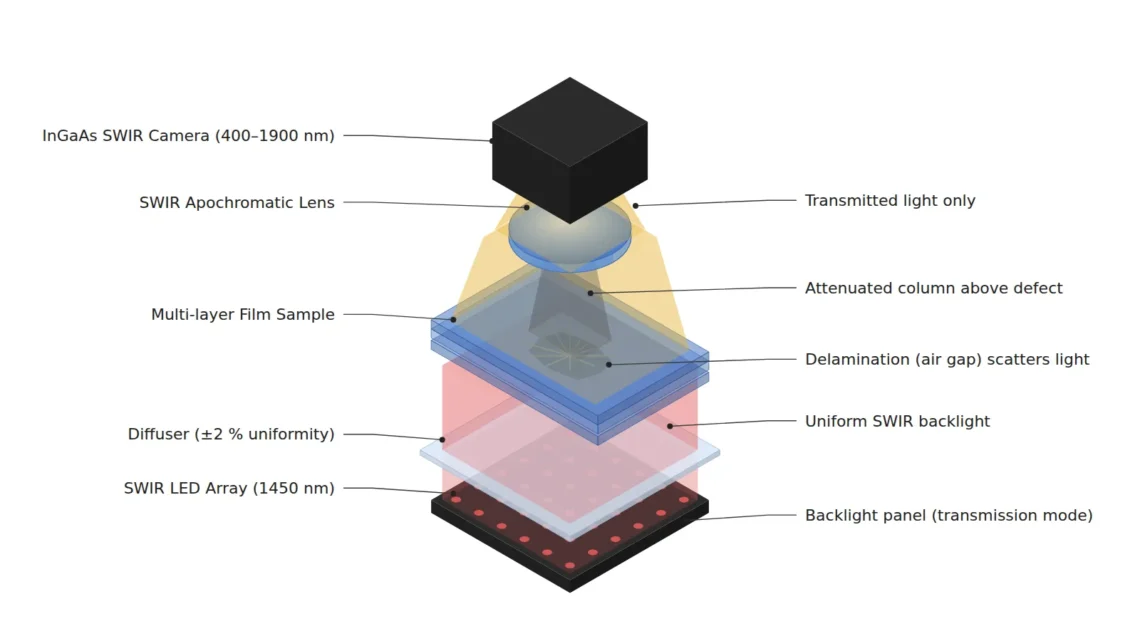
Once the print fades, the lifting appears on the transmission image as a shadow cast by an air layer. An air gap between film and resin adds two boundaries for the light to cross, and each boundary at a refractive index of 1.5 sends 4 % of the light back by Fresnel reflection6. Counting the light that bounces between the two surfaces, transmission is 92.3 %, so the lifted spot is 7.7 % darker than its surroundings. That value holds when the gap is thicker than the coherence length, the distance over which light can interfere with itself, and for a 1,450 nm LED with a 100 nm bandwidth that length is about 21 μm.
When the gap is much thinner than that, the reflections from the two surfaces interfere and the contrast swings with the gap thickness. By calculation, a 0.1 μm gap darkens by 12.6 % at 550 nm but only by 3.0 % at 1,450 nm, and a 0.05 μm gap by 4.8 % and 0.8 %. A thin lift actually looks darker in visible light. That runs against intuition. So on this cover I see the job of SWIR as erasing the print more than darkening the lifting. Even with the print out of the way, a lift that sits thinner than 0.1 μm is a signal of less than 3 %, and what hides that signal is the open question.
Moisture by the ratio of two wavelengths, lifting by one
Moisture is caught by a different method from lifting. Since water absorbs 25 times more at 1,450 nm than at 1,200 nm, dividing one image by the other leaves only the moisture dark in the ratio image. A 10 μm layer of water absorbs 3.1 % of the light at 1,450 nm and 0.13 % at 1,200 nm, so the ratio drops by 3.0 %. With the ratio image noise taken as 0.5 % and three times that, 3σ7, as the threshold, moisture is caught from a thickness of about 5 μm.
The same ratio image erases the lifting. The Fresnel reflection of an air gap barely depends on wavelength, so both images darken by the same 7.7 % and the division gives 1. Changes that affect both wavelengths equally, such as backlight nonuniformity, disappear as well. Because the two LEDs are separate devices, though, any small difference in how their light spreads stays behind as a pattern after the division.
The decision is therefore split between two images. Lifting and particles are searched on a single 1,200 nm image, where water absorbs weakly, and moisture on the ratio image. Try to see everything on one 1,450 nm image and both moisture and lifting come out dark, with no way to tell them apart. Two images are needed. My rule is that the decision design for SWIR transmission inspection starts from a table of which defect each wavelength is responsible for.
At 1,450 nm a 3.45 μm pixel sits inside the diffraction blur
With the percentages counted, it is time to count how many pixels the defects fill. The IMX992 that Sony announced on November 28, 2023 joins an InGaAs light-receiving layer to a silicon readout circuit with a Cu-Cu connection8, shrinking the pixel to 3.45 μm in a 5.32 MP sensor with 2,592 × 2,056 px that responds from 0.4 to 1.7 μm. One sensor can take both visible and SWIR light, so a design that switches only the lighting to get two images on the same optical axis is also possible.
My rule is to cover a 100 μm particle with at least three pixels, so one pixel must cover 33.3 μm or less on the cover, and 2,592 px gives a field of view of 86.4 × 68.5 mm. Widen the field to 120 mm and the pixel grows to 46.3 μm, leaving the particle on only 2.2 pixels. That falls short of the rule. Making the 0.1035 magnification with a 35 mm lens puts the WD9 from lens to cover at about 373 mm (thin-lens approximation).
The pixel count alone looks sufficient, but lens diffraction grows with the longer wavelength. At 1,450 nm the Airy disk10 of an F/4 lens is 2.44 × 1.45 × 4, or 14.2 μm across, 4.1 pixels. The blur is larger than a pixel. At the same F/4 the blur was 5.4 μm at 550 nm, so it has grown 2.6 times. Calculating an opaque 100 μm particle with this blur and the pixel size included, the darkest pixel is 77 % darker than the background, against 91 % at 550 nm. Stop down to F/5.6 and it becomes 60 %; open up to F/2.8 and it becomes 85 %.
14.2μm
Airy disk diameter at 1,450 nm and F/4 (4.1 pixels)
86.4mm
Field width that keeps a 100 μm particle on 3 pixels (2,592 px)
77%
Darkness of an opaque 100 μm particle (91 % at 550 nm)
In the numbers, diffraction does not make the particle slip through, but it shaves its darkness and narrows the gap to the threshold. On this cover I would not stop down past F/4, and I would also confirm that the depth of field11 at F/4, about 5.7 mm, covers particles anywhere in the cover thickness. The lens has to be a product whose transmission and focus are verified in the SWIR band. A lens made for visible light, used as it is, loses SWIR to its coatings and shifts focus with wavelength.
Lighting nonuniformity survives the flat-field division
In transmission inspection, backlight nonuniformity lands on the image in the same shape as a defect. On a backlight with ±10 % uniformity, a lift that is 7.7 % darker cannot be told from a valley in the nonuniformity, let alone the 3 % of a 0.1 μm lift. The figure is a concept diagram of how the same lifting signal changes on the two backlights.
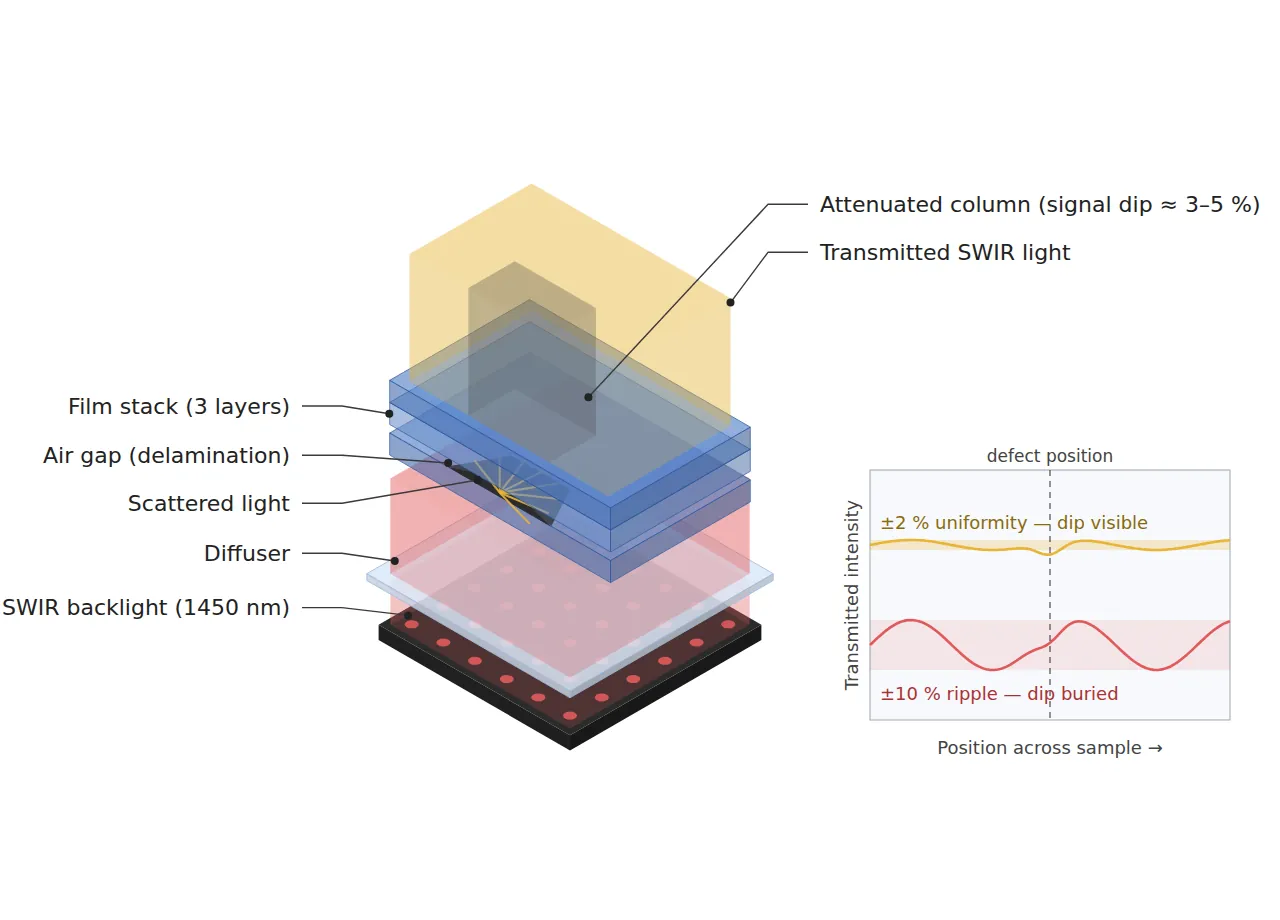
On the upper curve, the ±2 % backlight, the lifted spot shows as a clear dip, and on the lower curve, the ±10 % ripple, the same dip is buried in the middle of a wave. The 3 to 5 % in the figure is close to the case of a thin gap with interference mixed in; a thick gap brings it up to 7.7 %. The standard way to remove nonuniformity is flat-field correction12, which divides by a reference image without defects to strip out the shape of the backlight.
If division removed the nonuniformity completely, hardware uniformity would not matter, but after the reference image is taken, the shape of the nonuniformity can drift with LED temperature and aging. If that drift is 20 % of the nonuniformity, a ±10 % backlight still leaves ±2 % after correction, while a ±2 % backlight leaves only ±0.4 %. A 7.7 % signal against ±2 % nonuniformity has less than four times the margin, and the 3 % of a 0.1 μm lift becomes the same size as the nonuniformity. Then the two cannot be told apart. That is why I pin ±2 % uniformity down as a hardware specification; software correction cannot stand in for lighting nonuniformity.
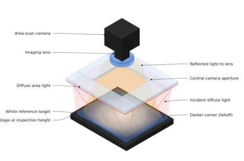
When the illumination budget is tight, buying uniformity with a thicker diffuser costs light, and a longer exposure costs tact time. Both have a price. I would choose to make the emitting area one margin larger than the 86.4 × 68.5 mm field of view, pushing the zone where brightness sags at the edges outside the field. When LEDs of the two wavelengths are mixed on one board, matching the way their light spreads sets the floor for moisture detection.
One cover, one SWIR setup table
Putting the numbers into one table lines up the defect each wavelength takes on with the hardware conditions that protect it. Particles, lifting and moisture each have their own contrast and their own threshold, and that is what divides the rows.
| Item | Value | Condition · basis | In plain words |
|---|---|---|---|
| ① Minimum defect size (μm) | Particle 100 μm across, film lift 500 × 500 μm, moisture 200 μm across · 5 μm thick | Particle on 3 pixels (33.3 μm/px). Lift contrast 7.7 % (thick gap) to 3.0 % (0.1 μm gap at 1,450 nm). Ratio drop of 3.0 % for 10 μm of water | Each defect darkens by a different amount |
| ② Lighting | 1,200 nm and 1,450 nm transmission backlights, uniformity within ±2 % (measured before correction), emitting area one margin larger than the field | ±0.4 % after correction if the nonuniformity shape drifts by 20 %. Differences in how the two LEDs spread remain in the ratio image | Division does not erase all the nonuniformity |
| ② Camera · lens · WD | IMX992-class 5.32 MP (2,592 × 2,056 px, 3.45 μm, 0.4 to 1.7 μm), 35 mm SWIR-rated lens at F/4, field of view 86.4 × 68.5 mm | WD of about 373 mm must be secured (thin-lens approximation). Airy diameter 14.2 μm at 1,450 nm (4.1 pixels), depth of field about 5.7 mm | The diffraction blur is larger than the pixel |
| ③ Algorithm parameters | Flat-field correction per wavelength, single 1,200 nm image (particles · lifting), 1,450 / 1,200 ratio image (moisture) | Threshold 3σ (σ re-estimated from 30 good parts), particle connected region of 9 pixels or more, lift connected region of 100 pixels (about 0.11 mm²) or more | Each wavelength takes on different defects |
The first thing this table says is that if the ±2 % of ② lighting is not held, the 3 % signal of a 0.1 μm lift stays the same size as the nonuniformity, whatever camera is fitted. Particles, on the other hand, keep a wide distance from the threshold even with their darkness shaved to 77 % by diffraction, so holding the aperture at F/4 is enough to protect them. For moisture, matching the spread of the two LEDs sets the threshold.
SWIR is plainly the wrong tool in some places. If the defect lives only in surface shape, like a scratch or a dent, transmission brings no advantage, and angled visible lighting or deflectometry does better. At a short tact time with a tight illumination budget, SWIR lighting easily becomes the bottleneck for exposure time, so if there is any room to create contrast in visible light, that route is more economical. If the resin and ink show no absorption difference in SWIR either, changing the wavelength gains nothing. SWIR transmission varies strongly with additives, pigments and thickness for each material, so which route fits cannot be guaranteed before a sample test.
Building the optics falls to the vision engineer, but whoever chooses the ink and film can help with the first row of this table. Print the pattern with inks free of carbon black and the lifting is likely to show in SWIR; print the same pattern in carbon black ink and that spot stays hidden to the end. If you are writing the purchase spec, I recommend putting it on the first line that the backlight uniformity specification governs the detection floor more than the camera pixel count does. This article explains technology and is not investment advice. See our Disclaimer.
Field Note
To bring SWIR to this cover, I would first place one printed film sample on 1,200 nm and 1,450 nm backlights, before choosing a camera, and see how many percent the pattern fades. If the pattern remains, I would put the ink conversation ahead of the camera specification. Next I would measure the backlight nonuniformity with a defect-free cover before correction, then shoot again a few hours after the reference image and check that the correction residual stays within ±0.4 %.
Field Checkpoints
Once the printed sample and the correction residual have been checked, check the items below.
- Is a WD of about 373 mm from lens to cover (35 mm lens, 86.4 mm field of view) actually available, clear of the backlight housing and fixtures? (a distance measured inside the equipment in place of a drawing value)
- Does a 100 μm particle land on at least three pixels? (widening the field to 120 mm cuts it to 2.2)
- Have the resin, film and ink of an actual lot been shot in transmission at 1,200 nm and 1,450 nm? (with samples in place of generic datasheet values)
- Is the lens verified for transmission and focus in the SWIR band, with the aperture no smaller than F/4? (stopping down enlarges the diffraction blur)
- Has the backlight uniformity been measured within ±2 % on the raw image before correction? (the residual that correction cannot remove scales with the uniformity)
- Do the LEDs of the two wavelengths spread their light in the same shape? (if not, a pattern remains in the ratio image)
- If one sensor captures both visible and SWIR, has the difference in focus position between the two wavelengths been checked?
Frequently Asked Questions
Can a visible-light camera see SWIR once its infrared-cut filter is removed?
It cannot. Removing the filter lets in near-infrared light up to around 1 μm, which silicon can receive, but beyond the silicon cutoff of 1,107 nm the pixels do not respond. The 1,450 nm band that separates moisture and the bands from 1,200 nm upward used to erase the print are visible only with another light-receiving layer such as InGaAs. Some inks may already fade in the near infrared, so testing 850 nm or 940 nm lighting with a silicon camera first is a cheap first step.
Does a thick cover push particles out of focus?
With a 3 mm cover, refraction makes a particle on the back face appear at a shallower depth of about 2 mm (thickness ÷ 1.5 at a refractive index of 1.5). The depth of field at F/4 is about 5.7 mm, so particles on both the front and back faces of the cover fall inside it. Thicker resin also absorbs more SWIR, though, so transmission at each thickness has to be measured on samples.
Glossary
- [1] Bandgap bandgap
The minimum energy a semiconductor needs to turn light into electricity. Dividing 1,240 by the bandgap in eV gives the longest wavelength it can receive, in nm. ↩ - [2] SWIR short-wave infrared
Infrared light in the band of roughly 0.9 to 1.7 μm, longer than visible light. It records the reflection and transmission of lighting more than the heat objects give off. ↩ - [3] Film insert molding FIM
A process that places a printed film in the mold first and then molds resin behind it so the two become one part. Where film and resin do not fully bond, the film lifts. ↩ - [4] InGaAs indium gallium arsenide
A compound semiconductor of indium, gallium and arsenic that receives light up to about 1.7 μm and is widely used as the light-receiving layer of SWIR cameras. ↩ - [5] Absorption coefficient absorption coefficient
A value that shows how quickly light fades as it passes through a material. Transmission is calculated as exp(−absorption coefficient × thickness). ↩ - [6] Fresnel reflection Fresnel reflection
Reflection in which part of the light turns back at the boundary between two materials of different refractive index. At a boundary between index 1.5 and air it is 4 % at normal incidence. ↩ - [7] 3σ three sigma
A way of setting the threshold at three times the standard deviation σ that describes how good-part images wander. If the wandering follows a normal distribution, good pixels rarely cross the line. ↩ - [8] Cu-Cu connection Cu-Cu connection
A bond that electrically joins two chips by pressing their copper pads directly together. Because the contacts can be made small, it is used to shrink the pixel pitch. ↩ - [9] WD working distance
The distance from the lens to the surface being inspected. The value in the text uses a thin-lens approximation measured from the lens center. ↩ - [10] Airy disk Airy disk
The disk that light spreads into after passing a circular aperture, unable to gather into a single point. Its diameter is 2.44 × wavelength × F-number, so it grows with longer wavelengths and smaller apertures. ↩ - [11] Depth of field DOF
The front-to-back range that can be treated as in focus. The value in the text takes the permissible circle of confusion as two pixels (6.9 μm). ↩ - [12] Flat-field correction flat-field correction
A correction that divides the inspection image by a defect-free reference image to strip out brightness patterns made by the lighting and lens. If the pattern changes after the reference is taken, the difference remains. ↩
References
- Sony Semiconductor Solutions, Sony Semiconductor Solutions to Release SWIR Image Sensor for Industrial Applications with Industry-Leading 5.32 Effective Megapixels (press release, November 28, 2023; IMX992 · IMX993, 3.45 μm pixels, 0.4 to 1.7 μm, Cu-Cu connection)
- M. Segelstein (1981), optical constants of water, as compiled by the Oregon Medical Laser Center: segelstein81.txt (31.5 /cm at 1,449 nm, 1.26 /cm at 1,199 nm)
- TriEye Ltd., US patent US11063079B2, Germanium based focal plane array for the short infrared spectral regime (priority January 9, 2018; filed January 2, 2019; granted July 13, 2021)
- TriEye Ltd., US patent US12100725B2, continuation under the same title (priority January 9, 2018; filed May 31, 2023; granted September 24, 2024)
- Teledyne FLIR, LLC (original assignee FLIR Systems, Inc.), US patent US7655908B2, Enhanced vision system sensitive to infrared radiation (priority March 5, 1999; filed September 1, 2006; granted February 2, 2010)
- Formulas: cutoff wavelength (nm) = 1,239.84 ÷ bandgap (eV), air-gap transmission = (1 − R)² ÷ (1 − R²) (R = 0.04), thin-gap reflectance = 2r²(1 − cos δ) ÷ (1 + r⁴ − 2r² cos δ) (r = 0.2, δ = 4π × gap ÷ wavelength), coherence length ≈ wavelength² ÷ bandwidth, moisture transmission = exp(−absorption coefficient × thickness), pixel resolution = particle diameter ÷ 3, WD ≈ f × (1 + 1/m), Airy diameter = 2.44 × wavelength × F-number, depth of field ≈ 2 × F-number × permissible circle of confusion × (1 + m) ÷ m², correction residual = uniformity × drift fraction of the pattern
Related reading — In SWIR, One Stop Down Erases a 3.4 μm Pixel · Vision Types Split First by Wavelength and Pixel Size · An 850 nm Band-Pass Filter Erases Factory Lights but Leaves Sunlight

Noctvision
An engineer who has handled mechanical design and project management for production equipment since 2005. Here I work through the cameras, lenses and lighting that go into equipment with formulas and public data, and record the assumptions and sources alongside the numbers.


You May Also Like
The Cost of Switching Between Dark-Field and Coaxial with Software-Defined Lighting
Changing the Sensor Means Recalculating the Illumination