In the Age of 8K Line-Scan Cameras, the Lens Still Sets the Ceiling on Inspection Resolution
If you run full inspection on surface-mount PCBs on an SMT line, this scene won’t be unfamiliar. On one specific lot, over and over, solder bridges or micro-cracks slip past the inspection machine into downstream processes, and in bad cases all the way to the customer. Trace the cause and, more often than not, the camera has already been upgraded to an 8K-class line-scan unit. When raising pixel count doesn’t reduce leakage, that’s a signal the bottleneck isn’t the sensor — it’s somewhere else.
A defect not caught at the early inspection stage grows exponentially more expensive to handle as it moves through further processes. As the 1-10-100 rule commonly cited in quality control puts it, the cost of catching something at inspection versus discovering it after shipment differs by an order of magnitude, not just a fraction. And yet in the field, equipment is still often re-selected on the assumption that “raising pixel count will reveal smaller defects.” To cut to the conclusion: the effective resolution ceiling of an inspection system is set not by sensor pixel count, but by the lens’s MTF (modulation transfer function) and lighting conditions. This piece uses a recently released 8K line-scan/NIR camera as an example to lay out how to re-examine the optical setup on a PCB-inspection standard.
Defining the Minimum Defect Size to Detect (µm) — Spatial Frequency, Not Pixel Count
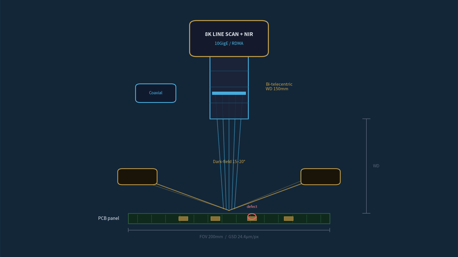
The minimum defect size an inspection system can actually detect is defined by GSD (Ground Sample Distance, the real-world size per pixel) and Nyquist sampling criteria. GSD is FOV (field of view, mm) divided by the sensor’s effective pixel count, and to reliably distinguish a single defect from noise, you typically need at least 2–3 pixels of width across it.
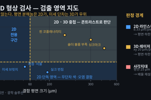
For example, capture a 200 mm FOV with an 8,192-pixel line-scan sensor and GSD comes out to about 24.4 µm/px. On a 2-pixel Nyquist basis, that computes to a theoretical detection limit of 48.8 µm — but that only holds on the premise that the lens delivers sufficient contrast (typically 30% or higher) at that spatial frequency. If the lens’s resolving power can’t support that spatial frequency, contrast gets crushed even though the defect exists on the pixel grid, and effective resolution always comes out worse than the calculated value. The table below organizes, by defect type, the minimum detection size that needs to be caught in practice and the lens spatial-frequency spec required to satisfy it.
| Defect type | Minimum detection size (µm) | Basis for calculation | Required lens spatial frequency (lp/mm) |
|---|---|---|---|
| Solder bridge / micro-crack | 50 | GSD 24.4 µm/px × 2px basis | ≥ 20 lp/mm (contrast 30%+) |
| Solder-mask pinhole | 75 | GSD 24.4 µm/px × 3px basis | ≥ 15 lp/mm |
| Foreign matter (particle) | 100 | Low-contrast-corrected 4px basis | ≥ 12 lp/mm |
| Plated-pin scratch (specular) | 30 | 2px basis + dark-field contrast correction | ≥ 30 lp/mm |
As the table shows, the minimum detection size for each defect type is only achieved when a lens is secured that actually delivers the corresponding spatial frequency — not simply by pixel count. Even with an 8K sensor, if the lens can’t hold contrast at 20 lp/mm, that line’s effective minimum detection size retreats from the table value to wherever the lens’s MTF curve satisfies 30%.
Optical Setup — Matching Lighting Condition to Lens Spec
Before settling on a solution, the target surface’s material and reflectivity must always be checked first. Even on the same PCB panel, a solder joint is a glossy metal surface dominated by specular reflection, solder mask is a matte surface dominated by diffuse reflection, and plated connector pins combine curvature and specular surfaces to produce pronounced diffuse scattering. Different materials call for different lighting methods.
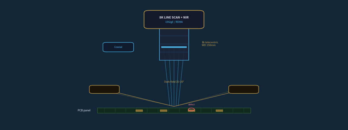
Coaxial epi-illumination is favorable for a solder joint dominated by specular reflection. Because it returns the specular light off a flat reflective surface straight back to the camera, only a crack or foreign matter that deflects the reflection direction stands out as relatively dark or bright. Conversely, for a defect where a fine step creates scattered light — such as a scratch on a plated pin or a silkscreen-print edge — low-angle dark-field illumination maximizes contrast. For a surface with inherently low visible-light contrast, like matte solder mask, combining an NIR (near-infrared) channel to boost contrast has become common practice recently, in step with the release of combined line-scan/NIR sensors.
The lens should be considered on a telecentric basis by default. It suppresses perspective error, keeping distortion manageable at 0.1% or below, and magnification error from subject-distance variation stays small. That said, a material like a plated connector pin, where curvature and specular surface overlap, can be difficult to fully control diffuse reflection on with coaxial lighting alone, so the final lighting angle and intensity cannot be confirmed before sample testing. And whatever lens/lighting combination is chosen, securing WD (Working Distance) is a separate item that must always be specified. If WD is insufficient, there’s simply no physical space to angle lighting in the way you need, and a dark-field setup that works on paper becomes impossible to implement on the actual line.
| Target material / defect | Lighting method | Illuminance (lx) | Lens spec | WD (mm) | Notes |
|---|---|---|---|---|---|
| Solder-joint crack/bridge | Coaxial epi-illumination | 25,000–35,000 | 0.5x bi-telecentric, distortion<0.05% | 150 | Glare reduced with a paired polarizer |
| Plated connector pin scratch | Low-angle dark-field (15–20°) | 40,000–60,000 | 1.0x telecentric, distortion<0.1% | 100 | Heavy diffuse reflection — sample testing recommended first |
| Solder-mask pinhole/foreign matter | Diffuse coaxial + NIR (850nm) | 15,000 | Standard FA lens f=25mm, distortion<0.3% | 80 | Low-contrast correction for matte surface |
| Molded connector housing joint crack | Low-angle dark-field (10–15°) | 35,000 | 0.35x telecentric | 200 | Extra WD margin needed for curved area |
As the table confirms, lighting method and WD requirements differ entirely by material even within the same line. A design that tries to cover every defect type with one lighting set inevitably becomes a compromise that sacrifices detection rate on specific defect types.
Algorithm Parameters — What Comes After the Optics Are Aligned
Algorithm parameters only become meaningful once the optical setup is aligned. Software image processing alone cannot fully cover structural hardware optical-setup defects such as lens distortion, insufficient MTF, or uneven lighting. However sophisticated the contrast correction in preprocessing, spatial-frequency information the lens never delivered in the first place simply doesn’t exist in the image.
Assuming the optics are aligned, defect-candidate detection defaults to setting the threshold at 3σ of the background-contrast gray-value difference (ΔGV). On an 8-bit basis, roughly ΔGV 12 becomes the boundary separating background noise from defect signal, and this value needs to be periodically recalibrated by measuring the actual lot’s noise distribution.
| Processing stage | Parameter | Recommended value | Purpose |
|---|---|---|---|
| Preprocessing | NIR-visible weighted-blend ratio | NIR 0.6 : Vis 0.4 | Boosting contrast on low-contrast surfaces |
| Defect-candidate detection | ΔGV threshold | Background 3σ (8-bit basis ΔGV≥12) | Noise-defect separation |
| Morphological filter | Minimum blob size | 3px × 3px | Removing sub-Nyquist noise |
| Edge detection | Sobel kernel | 5×5, directional threshold in 22.5° steps | Separating directional scratch-type defects |
| Classification | Defect confidence cutoff | 0.85 | Prioritizing false-detection suppression |
Counterpoint — When Raising Sensor Resolution Is the Favorable Approach
The principle that the lens sets the ceiling doesn’t always make a sensor upgrade meaningless. For a large PCB panel or a large-area molded part where FOV itself can’t be reduced, or a line running so fast that splitting FOV across more cameras isn’t practical, an 8K-class large-area sensor delivers a real gain. On a line that has already resolved the bandwidth bottleneck with an interface like 10GigE/RDMA, investing in the sensor can take priority over redesigning the lens. Even then, though, if the lens spec can’t support the new sensor’s pixel pitch, the effective return on that investment stays limited.
Field Checkpoints
Please confirm the following items before placing an equipment order.
- Has the target surface’s reflectivity been pre-measured by material, separated into specular, diffuse, and heavily diffuse reflection?
- Is WD (working distance) secured at 100 mm or more, with physical room to adjust the dark-field lighting angle — confirmation required?
- Has it been confirmed via chart that lens distortion/MTF spec actually satisfies the required spatial frequency (lp/mm)?
- Can interface bandwidth (10GigE/RDMA, etc.) handle the line speed without becoming a bottleneck?
- Has the ΔGV threshold been recalibrated against the actual lot’s noise σ?
If any of the five items above is difficult to confirm with certainty, send a sample specimen first and we can review it together starting from the optical-setup stage.


You May Also Like
The Line-Scan Camera You Picked by Line Rate Alone — Why It Still Misses Defects: TDI and the Resolution Design Relationship
Liquid Lens Autofocus: Solving the Focus Problem on High-Mix, Low-Volume Production Lines