The Lens Comes Before the AI — Optical Setup Design for PCB Inspection
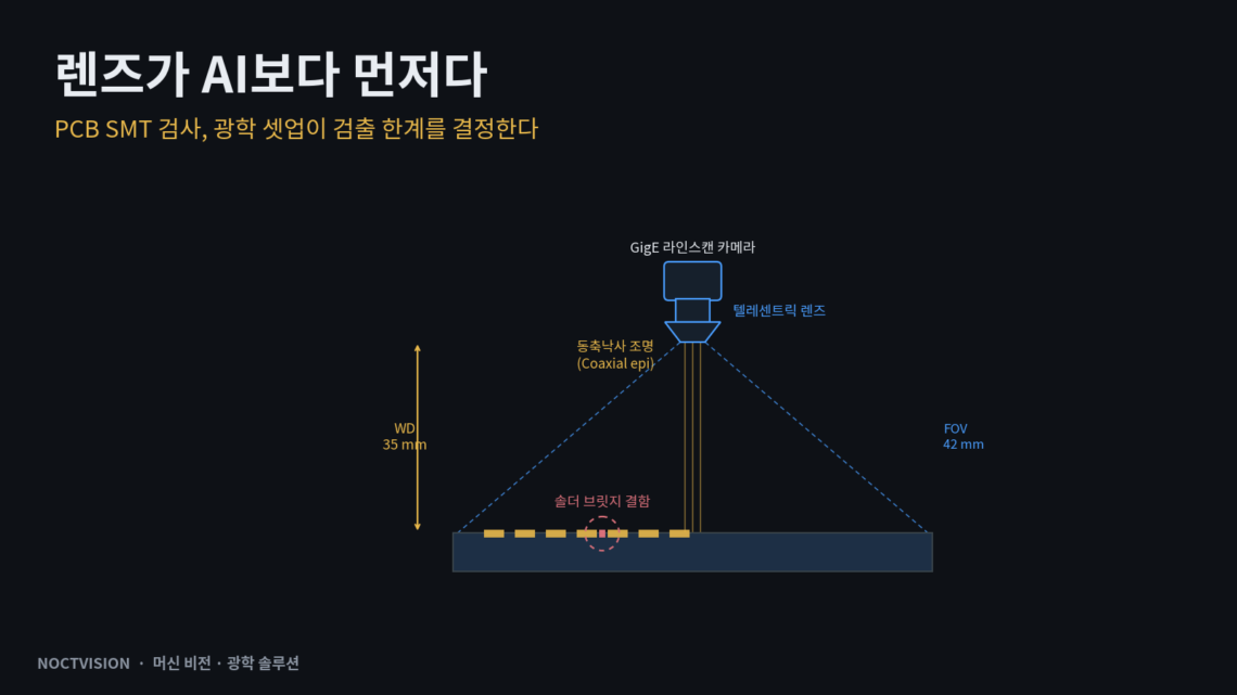
You’ve probably had this experience: your PCB surface-mount (SMT) line’s AOI passes thousands of boards a day, then suddenly starts missing solder bridges on one specific lot only. Most inspection engineers suspect the AI detection model first at this point. They add retraining data, adjust thresholds, try a new architecture. But the cause that keeps turning up, again and again, on the actual line floor is usually somewhere else entirely — the lens sitting on top of the camera, and the angle of the lighting shining on it.
Leave this defect unaddressed and the price is clear. A bridge that actually exists slips past the AOI and survives past reflow, and the field defect comes back as a far more expensive recall cost. Go the other way and narrow the judgment threshold to avoid missing anything, and false detections spike, repeatedly stopping the line and pulling in rework labor. The embedded-vision industry has recently made the same point: the lens is the gatekeeper of data quality, and optimizing the optical system pays off more than model tuning does. This piece translates that view into a practical standard for PCB SMT inspection, laying out why the optical setup needs to be checked first, and a concrete matching table.
Why the Lens Comes First — The Gatekeeper of Data Quality
If the image the optical system produces has already lost a defect’s geometric information, no algorithm bolted on afterward can restore information that isn’t there. That’s because, first, lens distortion and chromatic aberration are only partly offset by post-processing correction — the sub-pixel edge-position information itself is already crushed at the moment of capture. Second, if the lighting angle doesn’t match the target surface’s reflective characteristics, contrast never gets generated in the first place, and no matter how sophisticated the filtering, you can’t manufacture a signal that isn’t there. Third, because an AI model is only robust within the distribution of its training data, if optical conditions wobble lot to lot, you can easily fall into an endless loop of retraining just to hold the detection rate.
Recent embedded-vision commentary has indeed recommended ultra-low-distortion, telecentric lenses as the priority for industrial inspection optics. The bottom line: when your false-detection rate starts wobbling, the first thing to open isn’t the model weights — it’s the lens spec sheet.
Start With the Target Surface’s Material and Reflectivity
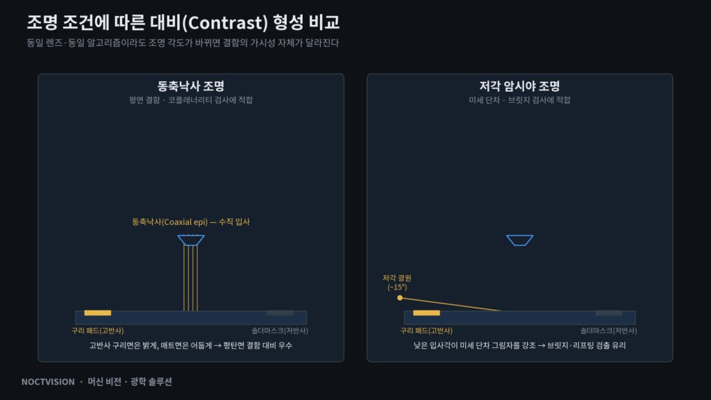
Before proposing a solution, the order is to check the target’s surface material and reflectivity first. That’s because even a single PCB contains three optically distinct surfaces at once. Copper pads are a highly reflective specular surface, solder mask is a low-reflectivity matte surface, and silkscreen ink is a semi-translucent scattering surface. Under the same lighting condition, these three surfaces return light in different ways, so it’s not easy for a single lighting-and-lens combination to capture defects on all three surfaces at optimal contrast simultaneously.
Targets with especially heavy diffuse reflection, like a solder-ball surface, have reflective characteristics that shift with lot-to-lot oxidation state and flux residue. For a target like this, it’s hard to declare a specific lighting angle always optimal, and it should be stated up front that this cannot be confirmed before sample testing.
Skeleton Standard — Detection Size / Optical Setup / Algorithm Matching Table
Organized around three defect types commonly handled in PCB SMT inspection, the target detection size and the corresponding optical setup and algorithm parameters are as follows.
| Defect type | ① Minimum detection size | ② Optical setup (lighting/lens) | ③ Algorithm parameters |
|---|---|---|---|
| Solder bridge | 25 µm | Low-angle dark-field (approx. 15°) + telecentric lens, WD 35 mm, FOV 42 mm | Edge-contrast threshold 0.18, morphological closing 3×3 px |
| Component coplanarity (lifted lead) | 40 µm | Coaxial epi-illumination + 8K line-scan, resolution 8.3 µm/px | Sub-pixel edge fitting ±0.3 px, shadow-width-based height estimation |
| Silkscreen smear/contamination | 60 µm | Diffuse dome illumination + NIR band-pass filter | Local contrast normalization (CLAHE) + classifier confidence threshold 0.85 |
The implication is clear. The smaller the defect size, the more lighting angle and WD settings affect detection rate before algorithm parameters do, and for a target as fine as a 25 µm-class bridge, algorithm tuning only produces reproducible gains once the optical setup has been fixed first.
Camera Specs and Securing WD — Recent Equipment Trends
When reviewing line-scan camera specs, it’s essential to check not just resolution but also whether WD (Working Distance) is achievable. Recently released 8K line-scan cameras have eased the bandwidth bottleneck with 10GigE/RDMA interfaces, and global-shutter sensors with boosted NIR-band sensitivity have also been announced around the same time. But even with 8K-class resolution secured, if WD interferes with the line’s physical structure, no lens upgrade — however good — makes installation possible. When designing a new line, it’s recommended to review physical interference with the lighting housing and top-plate structure at the same time as selecting camera/lens specs, and settle WD first.
Where AI AOI Fits — Algorithm Optimization Comes After the Lens
None of this means the algorithm’s role is small. Recent AOI equipment has been evolving toward AI-based auto-recipe teaching and auto buy-off features that dramatically cut programming effort. And it’s also true that on an already-installed line where swapping out the entire optical system is difficult, algorithmic compensation such as multi-exposure fusion or HDR compositing can make up for a substantial portion of the gap. But this compensation is limited to targets without large reflectivity variation, and treating software image processing alone as capable of fully covering a hardware optical-setup defect is exactly the point this piece cautions against. The algorithm’s role is to read the contrast the optics already created more precisely — not to manufacture contrast that was never there to begin with.
Field Checkpoints
- Confirm first whether WD (working distance) is achievable without interference from the lighting housing or top-plate structure.
- Measure reflectivity differences across the inspection target’s surfaces (copper pad/solder mask/silkscreen), and don’t draw conclusions for lots with heavy diffuse reflection before sample testing.
- When the false-detection rate wobbles, re-check lens distortion and lighting angle before retraining the model.
- Document the minimum detection size baseline (µm) alongside the optical setup table to track recipe-change history.


You May Also Like
Programmable Multi-Angle Lighting and Edge AI Inference: Redrawing the Limits of PCB Micro-Crack Detection
Why the PoE Network Card Sets the Limit on Your Optical Setup in a Multi-Camera Inspection Line