The Defect Zone You Miss When You Switch to 3D Inspection
I often see lines that bring in a 3D camera and still don’t see missed detections go down. Usually it’s not an algorithm problem. It’s that the planar (xy) resolution of a 3D profiler is actually coarser than 2D line-scan — a fact nobody confirmed with numbers at the setup stage.
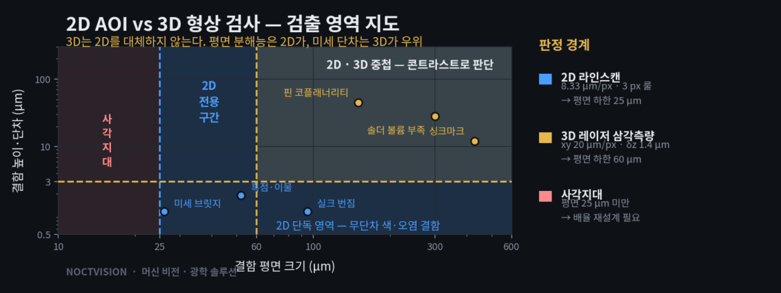
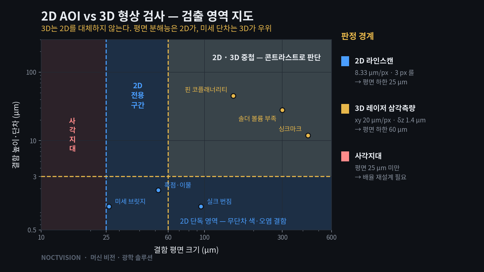
Leave this unaddressed and the entire defect group in the 25–60 µm width range — PCB micro-bridges, molded-part surface scratches — slips through wholesale. That’s because it’s a size that can’t land three or more points on the 3D pixel grid. Once leakage in this range starts, downstream rework labor and field-return costs quickly outrun the cost of the inspection equipment itself.
The solution is simple. Decide whether to adopt 3D not by defect size, but by the contrast actually achievable in 2D.
3D Is Not a Strict Upgrade Over 2D
The shift to 3D inspection is where the money is moving fastest right now. Machine-vision camera market outlooks project the overall market growing from $6.79 billion in 2025 to $20.9 billion by 2035 at an 11.89% CAGR, while 3D cameras are projected at a 15.83% CAGR — well ahead of the market average. Combined with inspection applications making up 38.6% of the total, a substantial share of that money is flowing into inspection lines.
But this growth figure creates a dangerous misunderstanding in the field: the assumption that “adding 3D replaces 2D.” Physically, that’s not the case. A laser-triangulation profiler’s xy resolution typically runs 15–20 µm/px — two to three times coarser than the 8 µm/px of a 2D line-scan on the same target. Height (z) resolution drops down into the 1 µm range thanks to sub-pixel peak detection, but the planar direction doesn’t get that benefit.
In other words, adopting 3D widens detection capability upward while narrowing it sideways. 3D is equipment for catching defects 2D can’t see — not equipment that also catches everything 2D used to catch. The moment you accept this asymmetry, the equipment-configuration discussion shifts from “what do we replace it with” to “which defect group goes to which channel.”
① Minimum Defect Size to Detect — The Floor Set by the 3-Pixel Rule
The first thing to check is the target’s surface material and reflectivity. A semi-matte surface like PCB solder resist and a strongly specular surface like glossy ABS molding produce completely different images under the same lighting. Material has to be settled before lighting can be settled, and lighting has to be settled before the numbers below mean anything.
The practical floor for stable detection is the point where a single defect spans at least 3 px. Apply a 7 µm pixel pitch to a 2D line-scan at 4,096 px, giving an object-side resolution of 8.33 µm/px, and you get a 34.1 mm FOV with a planar floor of 25 µm. A 3D profiler at 20 µm/px xy resolution gives a planar floor of 60 µm. In the height direction, at a 45° triangulation angle and 1/20 px laser-line sub-pixel precision, δz = (20/20) ÷ sin 45° ≈ 1.41 µm, so applying a 2x safety factor gives a step-height floor of 3 µm.
② Optical Setup and ③ Algorithm Parameters Matching Table
| Defect type | ① Minimum detection size | ② Optical setup (lighting / lens-WD) | ③ Algorithm parameters |
|---|---|---|---|
| PCB micro-bridge/open circuit | Planar 25 µm | Low-angle ring (dark-field) 8,000 lx / telecentric 0.84x, line-scan 4,096 px, WD 110 mm | Adaptive threshold ΔGV ≥ 8, minimum blob 3 px, morphological open 3×3 |
| PCB silkscreen smear | Planar 80 µm | Diffuse dome 5,000 lx / 23 mm focal length, 5 MP color, WD 200 mm | HSV S-channel threshold, area ≥ 9 px, Gaussian σ 1.2 |
| Molded-part black spot/foreign matter | Diameter 50 µm | Coaxial epi-illumination 3,000 lx + dome mixed / 34 mm focal length, 5 MP mono, WD 200 mm | ΔGV ≥ 12 after background subtraction, circularity ≥ 0.6 |
| PCB solder volume shortfall | Step 30 µm (planar 300 µm) | 3D laser triangulation θ 45°, 405 nm line / xy 20 µm/px, WD 90 mm | Residual ≥ 30 µm after reference-plane fitting, volume-integral judgment |
| Connector-pin coplanarity | Step 40 µm (planar 150 µm) | 3D laser triangulation θ 60° / xy 15 µm/px, WD 75 mm | Extract mean z of top 5% of pins, reference-plane deviation ≥ 40 µm |
| Molded-part sink mark | Depth 12 µm (planar 400 µm+) | Deflectometry pattern display / telecentric, WD 150 mm | Second derivative of slope map, curvature threshold 0.02°/mm |
The value worth watching in this table isn’t defect size — it’s WD. The WD on all three 3D triangulation rows runs short, at 75–90 mm. That’s because the structure that widens the triangulation angle to get height resolution requires the camera and laser to sit close to the target. 2D, by contrast, has room out to 200 mm. Clearance from jigs and handlers narrows by exactly that difference, so the decision to adopt 3D often comes down not to optical spec but to measured mechanical clearance.
The Branching Criterion Is ΔGV, Not Size
In an 8-bit image, set sensor noise σ at 1.5 GV and the contrast floor for stable detection is 3σ = 4.5 GV. If, even after optimizing lighting, a defect’s ΔGV still doesn’t reach twice that value, that defect group isn’t something more 2D algorithm tuning will fix. Conversely, routing a defect with plenty of ΔGV over to 3D just throws away resolution for nothing.
# 2D/3D routing decision — branch on contrast, not defect size
XY_2D_MIN, XY_3D_MIN, Z_3D_MIN = 25.0, 60.0, 3.0  # planar/step floors [um]
DGV_MIN = 4.5      # 3-sigma contrast floor at 8-bit noise sigma=1.5 GV

def route(xy_um, z_um, dgv):
    """xy: defect planar size [um], z: step height [um], dgv: gray contrast after lighting optimization [GV]"""
    if xy_um < XY_2D_MIN:
        return "Blind spot -- pixel resolution needs to go up (magnification redesign)"
    if dgv >= DGV_MIN * 2:              # Contrast already sufficient in 2D -> 3D not needed
        return "Keep on 2D"
    if z_um >= Z_3D_MIN and xy_um >= XY_3D_MIN:
        return "Route to 3D"             # has a step, but contrast doesn't come up in 2D
    return "Redesign 2D lighting and re-judge"  # a zone even 3D resolution can't cover
The last return value of this function matters most in practice. A defect that’s 25–60 µm in the plane but low in contrast won’t get caught even if you route it to 3D. The only remaining option is to redesign lighting angle and wavelength to actually generate contrast. The moment you assume software post-processing can make up for a shortfall in the optical setup, this zone stays permanently undetected.
When a 3D-Only Configuration Is Actually Favorable
Contrary to the argument so far, there are certainly conditions where dropping 2D and keeping only 3D is the better call. First, when surface color and material are uniform enough that color/contamination defects never occur in the first place and only shape deviation needs managing. Second, when plating unevenness or gloss variation makes the 2D threshold wobble lot to lot, accumulating false detections — height data is relatively insensitive to surface-reflectivity variation, so threshold stability is actually better. Third, when the governing spec itself is defined in dimensions or volume, leaving no basis for converting a gray value into a spec limit.
That said, for materials with strong specular or heavy diffuse reflection — mirror-finish plating, hairline-machined surfaces, semi-translucent molded parts — the judgment above doesn’t hold as-is. Because the laser line scatters beneath the surface, the height profile itself wobbles. For material groups like this, this cannot be confirmed before sample testing. Please measure the line profile’s peak width and standard deviation on an actual specimen first, before making the call.
Field Checkpoints
- Is WD secured? — A 3D triangulation head typically runs WD 75–90 mm. Confirm actual clearance from jigs, handlers, and existing brackets by measurement, not from a drawing. If there’s no margin and WD has to be increased, the triangulation angle shrinks and height resolution collapses right along with it.
- Measure 2D contrast — Before getting a 3D quote, measure ΔGV for the problem defect group across 100+ samples under the current lighting and check the histogram. If it exceeds twice 4.5 GV, 3D isn’t needed yet.
- Recalculate the planar floor — Multiply the proposed 3D head’s xy resolution (µm/px) by 3 to get the planar floor yourself, and compare it against your currently managed minimum defect spec. This one-line calculation prevents most post-adoption missed-detection incidents.
- Laser wavelength and material combination — 405 nm has shallow penetration, favoring semi-translucent resin; 660 nm scatters less, favoring metal surfaces. When you have a specimen, test both wavelengths together.
References
- SNS Insider, Machine Vision Camera Market Size 2026-2035 (2026-08-17) — market size and 3D camera CAGR data. View original


You May Also Like
When Specular and Matte Meet in One Frame: Reviving Contrast with HDR Multi-Exposure Fusion
Machine-Vision Inspection: Physics Comes Before Software