Is It Safe When the Average Latency Fits the Deadline? — Breaking Down the Edge Vision Inspection Latency Budget by p99
EDGE AI / ALGORITHM
When an edge vision inspection system is introduced, the first number reported is usually the “average inference time.” If the benchmark screen shows 9 ms, the inspection cycle is judged fast enough and the project moves to the next step. On the line, however, the moments when the decision signal arrives late come not from the average but from the tail. Inference is only one section of the full path from trigger to reject signal, and the fluctuation of the remaining sections is not captured by the benchmark.
Left unaddressed, the cost appears in a rare but critical form. When the decision signal misses the deadline at the reject point, that part passes through regardless of the decision result. A system that is late about once in 1,000 parts looks perfect on average metrics, but if that one part was defective, the inspection process has left only a record and let the defect escape. In a worse case, one late event pushes the queue and makes the following parts late as well, in a chain.
Before making the inference model faster, the solution is to measure each of the seven stages exposure → sensor readout → transfer → preprocessing → inference → post-processing → decision signal, and to allocate the per-stage budget on the worst case (p99) rather than the average. On top of that, throughput is managed with pipeline parallelization and the latency ceiling with a deadline margin, separately.
What the line remembers is not the average latency but the single time the deadline was missed.
1. The Latency Budget Is Not the Inference Time but the Sum of Seven Stages
Point. When discussing edge inspection latency, the reference interval should be not “from model input to output” but “from trigger input to decision signal output”.
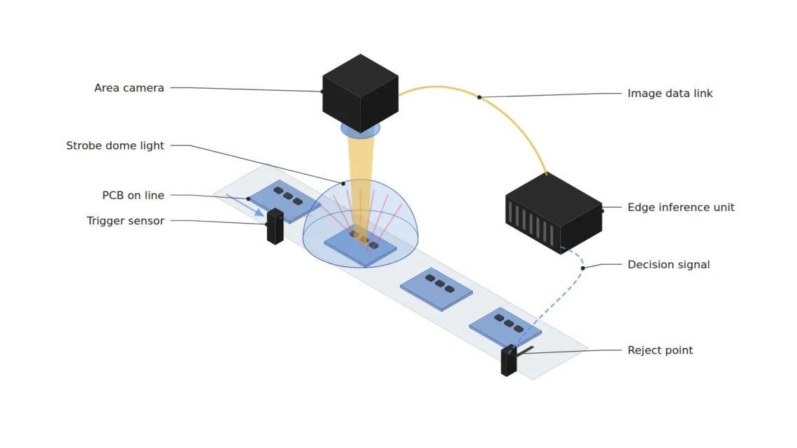
Reason. What the line requires is that the signal comes out before the part reaches the reject point. This deadline is set by dividing the distance between the camera station and the reject point by the part speed. Inside it are the optical and sensor section of exposure and sensor readout, the data path section of transfer, the compute section of preprocessing, inference and post-processing, and the signal section in which the operating system drives the digital output. Inference is one slot among them, and often not the slot with the largest fluctuation.
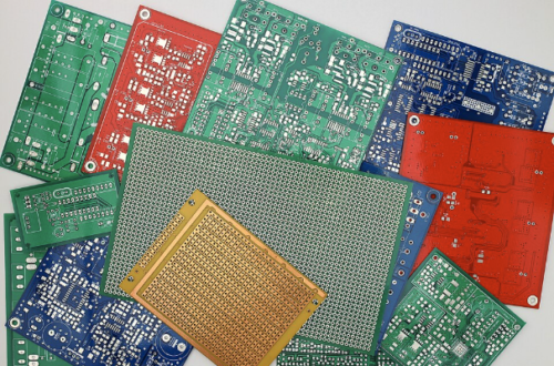
Example. As a design assumption, consider PCB inspection on a high-speed assembly line with a part speed of 300 mm/s and 18 mm from the camera to the reject point. The deadline is 18 ÷ 300 = 60 ms (calculated). The per-stage p50 values are exposure 0.03 ms, readout 8 ms, transfer 12 ms, preprocessing 3 ms, inference 9 ms, post-processing 1 ms, signal output 0.5 ms and so on, summing to about 33.6 ms. Looking only at the average, it is a comfortable system that barely exceeds half the deadline. At an exposure time of 30 µs, motion blur is 300 mm/s × 30 µs = 9 µm, only 0.45 px against a pixel resolution of 20 µm/px.
Point. Therefore the first table in the design review should be not the model benchmark but a seven-stage timestamp table. The control conditions of the part transport mechanism itself require a separate review. This article covers only the vision-side path from trigger to decision signal.
2. Why the Budget Must Be Allocated on p99, Not the Average
Point. The per-stage budget must be filled with measured p99 values, not p50, and their sum must leave a margin inside the deadline.
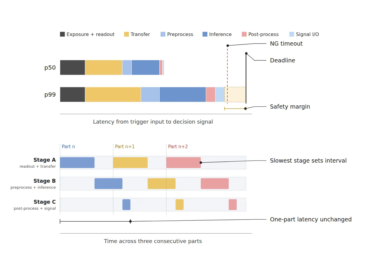
Reason. The distribution of each stage is not symmetric. Transfer has a long right tail from buffer contention and retransmission, preprocessing and inference from memory allocation and compute-unit contention, and signal output from operating system scheduling. The average dilutes this tail. Defect escapes, on the other hand, happen only in the tail. The simple sum of per-stage p99 values is a more conservative upper bound than the actual overall p99, but in correlated intervals where several stages slow down at once, such as a temperature rise or a load surge, the real latency actually approaches this bound.
Example. In the same PCB inspection, the measured p99 values (design assumption) grow to transfer 18 ms, preprocessing 6 ms, inference 15 ms, post-processing 3 ms and signal output 3 ms. Adding readout 8 ms and the exposure and trigger delay gives a sum of about 53.1 ms. The margin against the 60 ms deadline is 6.9 ms, a margin ratio of 11.5%, which barely clears the 10% design criterion. Compared with the p50 sum of 33.6 ms, the tail takes about 19.5 ms, and the largest increase within it comes not from inference but from transfer (+6 ms).
Point. The priority of countermeasures against budget overrun is not “the stage with the largest p50” but “the stage with the largest p99 − p50 gap”. Cleaning up transfer buffers and scheduling often pays off before model lightweighting does.
The first step in cutting the latency budget is finding not the slowest stage but the stage that fluctuates the most.
3. Pipeline Parallelization Raises Throughput but Does Not Cut Latency
Point. The latency deadline and the processing interval are different constraints, and pipeline parallelization solves only the processing interval.
Reason. If parts arrive every 40 ms and the p99 of serial processing is 53.1 ms, the processing of the next part is pushed back every time a tail event occurs. Even when the average of 33.6 ms is within the interval, the tail builds a queue, and the built-up queue lengthens the latency of the following parts in a chain. If the seven stages are grouped into three stages, “readout and transfer,” “preprocessing and inference,” and “post-processing and signal,” and run concurrently, what determines the processing interval becomes not the total sum but the single slowest stage.
Example. The p99 per stage is 26 ms for readout and transfer, 21 ms for preprocessing and inference, and 6 ms for post-processing and signal. Because the slowest stage at 26 ms is shorter than the 40 ms part interval, no queue builds up. However, the time one part takes from trigger to signal is still about 53.1 ms. If buffer copies are added between stages, it can even grow slightly. Even after parallelization, the deadline margin calculation has to be redone as it is.
Point. A timeout policy for cases in which no decision comes out until just before the deadline is also part of the budget. If there is no result by the point of deadline − margin, setting the default to reject (NG) so that “late decision = pass” never happens is the last safeguard against escapes. It should also be remembered that software optimization alone cannot cover a defect in the optical setup, for example motion blur caused by a long exposure.
4. Core Framework — Matching Table
| Category | Item | Specification / Parameter | Basis & Notes |
|---|---|---|---|
| ① Minimum defect size | PCB solder bridge | Width 60 µm or more | Design assumption. Occupies 3.0 px at 20 µm/px |
| ① Minimum defect size | Foreign particle on board surface | Diameter 100 µm or more | Design assumption. Occupies 5.0 px |
| ② Optical setup | Illumination | Diffuse dome light, strobe 30 µs, trigger-synchronized | Intended to suppress diffuse reflection from solder. Motion blur 9 µm (0.45 px, calculated) |
| ② Optical setup | Sensor | 2448 × 2048 px, pixel pitch 3.45 µm | Design assumption. Sensor width 8.45 mm (calculated) |
| ② Optical setup | Lens | Focal length 25 mm | Magnification about 0.172× (sensor width ÷ FOV, calculated) |
| ② Optical setup | WD (working distance) | 160 mm or more must be secured | Thin-lens approximation object distance about 170 mm (calculated). Verify by measurement including dome light height |
| ② Optical setup | FOV & pixel resolution | FOV 49 mm × 41 mm, 20 µm/px | 49 mm ÷ 2448 px = 20.0 µm/px (calculated) |
| ③ Algorithm | Latency deadline | 60 ms (18 mm ÷ 300 mm/s) | Design assumption. Measured from trigger input to decision signal output |
| ③ Algorithm | Sum of per-stage p99 | 53.1 ms, margin ratio 11.5% | Criterion: keep margin ratio at 10% or more. Derived from 10,000 or more per-stage timestamps |
| ③ Algorithm | Pipeline | 3 stages, longest stage p99 26 ms | Must be under the 40 ms part interval so that no queue builds up |
| ③ Algorithm | Timeout | Output NG if undecided at 54 ms | Deadline 60 ms − margin 6 ms. Blocks “late decision = pass” |
Table implication. The 60 µm solder bridge in ① is 3.0 px at the 20 µm/px of ②, sitting right at the detection floor, and the 0.45 px motion blur of the 30 µs strobe is acceptable within those 3 px. But if the latency budget runs short and a compromise is made such as extending the exposure to 60 µs to lower the illumination output, blur becomes 0.9 px and directly erodes the edge contrast of a 3 px defect. The latency budget and optical resolution are not independent; they are tied together by a single variable, the exposure time.
5. When the Opposite Approach Wins
- When the deadline is much longer than the part interval: If the reject point is far away and the deadline is several hundred ms or more, the benefit of per-stage p99 management is small. An average-based design with a single end-to-end timeout may be enough.
- Sampling inspection that does not use the decision immediately: For offline inspection whose results are used only for logs and statistical control, throughput and accuracy take priority over latency. Batch processing is more economical.
- Simple decisions whose computation can move inside the camera: When the computation is light, as in rule-based dimensional checks, a structure that removes the transfer stage cuts the tail more than pipeline splitting does.
For materials mixed with diffuse reflection such as solder surfaces, the required exposure and preprocessing load change with the illumination conditions, so the per-stage budget figures cannot be confirmed before sample testing.
Field Note
On a high-speed assembly line, there was a case where missed decisions were logged a few times a day even though the average decision time was about half the deadline. I suspected the model first, but after stamping timestamps at each of the seven stages and separating out p99, most of the tail turned out to come not from inference but from transfer buffer contention and signal output scheduling. After splitting into three stages and fixing a timeout 6 ms before the deadline to NG, the missed-decision records disappeared. Still, I find it hard to assert without measurement that the same configuration would hold for other boards and illumination conditions.
Field Checkpoints
- Is a WD of 160 mm or more secured by measurement — verify including the dome light housing height and the cable bend radius.
- Has the surface material and reflectance of the target been identified first — exposure and preprocessing load change with the degree of diffuse reflection on the solder surface.
- Are timestamps recorded for all seven stages from trigger input to decision signal output.
- Has the per-stage p99 been derived from 10,000 or more samples of continuous operation data — benchmark averages are not a basis for the budget.
- Does the p99 sum leave a margin of 10% or more against the deadline, and is the slowest pipeline stage shorter than the part interval.
- Is a timeout policy that outputs NG when undecided before the deadline implemented in the signal output stage.

Noctvision
A machine vision engineer who fits cameras, lenses, lighting, and image-processing algorithms together for a living. Years spent on continuous production lines, vibration, heat, and dust included, working through diffuse reflection, contrast, and resolution differences too fine for a spec sheet to capture inform every post here, closing the gap between theory and the shop floor. Off duty, that same eye for light and lenses goes into repairing fully mechanical vintage film cameras.


You May Also Like
Edge AI Inference Latency: The Camera Interface Decides Before the NPU Does — GigE Vision 3.0 RDMA and Disaggregated Inspection Architecture
In the Age of Deep-Learning Inspection, What to Check Before Camera Spec