Edge AI Inference Latency: The Camera Interface Decides Before the NPU Does — GigE Vision 3.0 RDMA and Disaggregated Inspection Architecture
Introduction — The NPU Changed, So Why Didn’t Throughput?
It’s a situation I run into often: a PCB SMT line’s edge-AI inspection controller gets upgraded to the latest NPU, yet the number of panels processed per second still falls short of target. In this situation, most people’s first suspect is the inference model or the NPU’s raw compute performance. But when you actually trace the bottleneck, the segment where the image crosses from camera to host memory — in other words, the camera interface’s CPU overhead — turns out to be the culprit more often than not.
Leave this bottleneck unaddressed and what happens is clear: you end up either lowering line speed to match the interface’s ceiling, or reducing inspection resolution to cut data volume — and detection headroom for 30 µm-class micro-defects shrinks right along with it. Fortunately, the GigE Vision 3.0 standard, officially ratified on April 17, 2026, opens a path to redesigning this segment itself through RDMA-based streaming (GVRSP).
Why the Camera Interface Becomes the Bottleneck
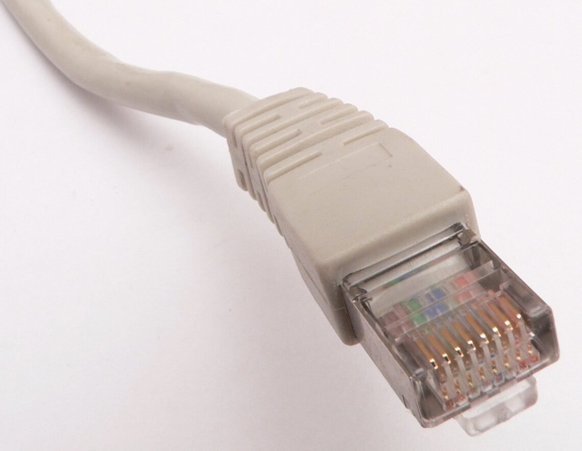
Conventional GigE Vision streaming has the host CPU receive and process every packet the camera sends over a software path, then copy it into application memory. With a single camera this isn’t much of a problem, but in a configuration like a PCB inspection line, where multiple GigE Vision cameras feed into one edge controller, CPU occupancy accumulates in proportion to camera count.
GigE Vision 3.0’s GVRSP bypasses this software path using RoCEv2 (RDMA over Converged Ethernet). By eliminating the copy step between application memory and OS buffers, measured tests have reported CPU occupancy dropping from the 50% range to under 10%, throughput exceeding 2 GB/s, and latency improving by roughly 80%. In a multi-camera GigE Vision 3.0 configuration, in other words, a significant portion of the frame budget was already being consumed at the interface segment before the edge NPU ever received the frame.
Disaggregated Edge Architecture: Why Separate Capture from Inference
Rather than cramming camera, preprocessing, inference, and judgment into a single controller, the architecture that separates these by role has been confirmed in real deployed cases at COMPUTEX 2026. When capture, analysis, and judgment are each handled by a different controller, the bandwidth and latency requirements of each segment can be designed independently, which makes it far easier to pinpoint where a bottleneck actually sits.
AAEON unveiled a disaggregated AI system that splits a PCB inspection pipeline into capture, analysis, and judgment stages across the UP Xtreme PTL, an Intel Xeon 6-based EATX-W890A workstation board, and an Intel Core Ultra Series 3-based BOXER-6650-PTH fanless controller. Even in a structure like this, though, if the interface between camera and capture controller is the bottleneck, no NPU downstream — however powerful — can make up for it; its performance simply gets buried. GigE Vision 3.0 RDMA is the first domino that has to fall for a disaggregated architecture to actually operate as designed.
The NPU Is Already Plenty Fast
That the edge NPU’s own compute performance isn’t the source of the bottleneck is also borne out by recently announced embedded-processor roadmaps. AMD’s Ryzen AI Embedded P100 series integrates 8–12 Zen 5 cores with an NPU rated up to 80 TOPS, targeting industrial machine-vision inspection PCs, and is currently sampling ahead of mass-production shipment in Q2–Q3 2026. The faster NPU compute capability grows relative to interface bandwidth, the further the bottleneck shifts toward the camera-to-host data-transfer segment. An investment that swaps out only the NPU, without GigE Vision 3.0 RDMA, is likely to land as no more than half a solution.
Core Skeleton Matching Table
The following is organized around a configuration inspecting micro-cracks and bridges on solder-fillet surfaces simultaneously with multiple cameras on a PCB SMT line. It should be noted up front that solder fillets are a strongly specular, glossy metal surface, so camera-interface improvement alone does not guarantee the detection rate itself.
| Item | Spec |
|---|---|
| ① Minimum defect size to detect | 30 µm (solder-bridge / hairline-crack baseline) |
| ② Optical setup | 4x 12MP (4096×3000) GigE Vision 3.0 cameras in a parallel configuration, 35 mm fixed-focal lens, F/4, WD 150 mm secured, FOV approx. 60×44 mm, coaxial epi-illumination + low-angle dark-field mixed lighting, pixel resolution approx. 14.6 µm/px |
| ③ Algorithm parameters | Frame rate 60 fps (16.6 ms frame budget), edge NPU inference model input 640×640 with inference latency under 8 ms, GigE Vision 3.0 GVRSP (RDMA over RoCEv2) streaming, target CPU occupancy under 10%, target throughput 720 MB/s or higher per camera (approx. 2.9 GB/s combined across 4 cameras) |
In this configuration running four cameras simultaneously, it’s difficult to sustain the target combined throughput (approx. 2.9 GB/s across 4 cameras) without GVRSP, which in turn means the interface segment eats into the 16.6 ms per-frame inference budget allotted to the edge NPU. Conversely, for a smaller line with only one or two cameras and a low required frame rate, where the necessary bandwidth stays within 1GigE-class territory (roughly under 100 MB/s), the cost of the NIC/frame-grabber replacement that adopting RDMA entails can be excessive relative to the bottleneck it actually relieves. This boundary condition varies with the actual line configuration, so it cannot be confirmed before sample testing.
What the Related Patents Show — A History of Resolving the Camera-Processor Bottleneck
This isn’t the first attempt to reduce memory copying between camera and processor. Three patents found on Google Patents trace the same underlying problem being solved differently across different eras.
- US20090027509A1 (Vision System With Deterministic Low-Latency Communication, published 2009-01-29) — an early case implementing deterministic low-latency communication between a vision system and peripheral devices via an EtherCAT interface.
- CN109089029B (Jinan University, published 2020-11-13) — an embedded transmission structure that raises GigE Vision interface image-transfer efficiency and lowers logic-resource occupancy, based on an FPGA and PHY chip.
- US20240406579A1 / granted as US12316981B2 (NXP B.V., filed 2023-08-01, published 2024-12-05) — a structure that feeds camera stream frames directly into the ISP without storing them in external memory, implementing the same directional goal as RDMA (minimizing memory copying) at the stream-processing stage.
What’s interesting is that all three patents pursue the same goal — “eliminating unnecessary memory copying between camera and processor” — but solve it at a different layer each time: deterministic communication in 2009, FPGA-embedded transmission in 2020, and direct stream-to-ISP in 2024. GigE Vision 3.0’s GVRSP is the standardized version of this lineage.
Field Checkpoints
- Has it been directly confirmed via spec sheet that the camera, frame grabber, and NIC all support GigE Vision 3.0 GVRSP (RDMA over RoCEv2)?
- When running multiple cameras simultaneously, has the required throughput (fps × resolution × bit depth × camera count) been calculated and actually compared against interface bandwidth?
- Is WD (working distance) secured? — Does the lens/lighting layout actually secure, within the line’s physical layout, the WD needed to satisfy the target FOV and resolution independent of the camera-interface change?
- For strongly specular solder/metal surfaces, since interface improvement alone doesn’t guarantee detection rate, has this been separately verified through sample testing?
References
- LUCID to Showcase New 8K Line Scan, NIR, STARVIS, and 3D RGB-D Cameras at VISION 2026 — Vision Systems Design
- RDMA Cameras and GigE Vision 3.0: High-Speed Streaming Standards — LUCID Vision Labs
- RDMA Technology in Vision Applications — STEMMER IMAGING
- Removing the CPU Bottleneck in High-Bandwidth Machine Vision — Quality Magazine
- COMPUTEX 2026 Announcement — AAEON
- Top AI Inference Chips for Edge Devices in 2026 — Kynix
- US20090027509A1 — Google Patents
- CN109089029B — Google Patents
- US20240406579A1 / US12316981B2 — Google Patents


You May Also Like
AOI Only Says “Defective” — How Vision Language Models Fill the Gap in Judgment Rationale
Detection Time Cut 65%, False Alarms Down 80%: How to Read the Two Numbers Behind Edge Fire-Detection AI