PCB and Semiconductor Surface Inspection: The 15–40µm Boundary the Human Eye Misses
I recently came across news, in the Korea Machine Vision Industry Association’s newsletter, of Vieworks’ preliminary results showing first-half 2026 operating profit up roughly 127% year over year. What caught my attention wasn’t the number itself, but the background behind it. Demand growth like this is, in the end, a signal that quality standards for micro-defects the human eye can no longer catch are accelerating across the entire industry.
Visual inspection still remains in PCB and semiconductor packaging lines. The problem is that 15–40 µm-class micro-scratches, solder bridges, and foreign matter sit outside the human eye’s practical resolving power. A leak comes back as field claims and line rework costs. The solution is a combination: an optical setup that makes the defect stand out, and algorithm parameters that don’t miss that signal.
The FOV-versus-resolution trap
Inspection design has to start from defining the minimum defect size. Widen the FOV, and the actual measured area per pixel grows, so a 15–40 µm-class defect gets crushed down to less than 1 px. It’s the same principle as a vintage film camera’s wide-angle lens widening the field of view while sacrificing detail. Fit a 300 mm-wide panel into a single field of view, and a bridge defect gets buried in background noise. FOV and resolution always have to start from working backward off the minimum detectable size.
Surface material and lighting strategy
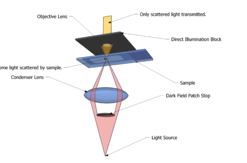
Before the solution, the target’s surface material and reflectivity need to be checked first. PCB solder mask is close to matte, so contrast holds up even with diffuse illumination, but a metallic-gloss surface like a solder ball has strong specular reflection, producing the opposite result. Low-angle dark-field illumination enlarges the shadow of a step to raise contrast, but on a plated surface with heavy diffuse-reflection variation, even a 5-degree difference in lighting angle can flip the result, so this cannot be confirmed before sample testing.
Lens and securing WD
When proposing a lens spec, whether WD is secured always has to be stated alongside it. On a semiconductor packaging line, interference with the handler or lighting module means that if WD is insufficient, it becomes difficult to fit a macro lens at the desired magnification. Catching a 25 µm defect at 3 px or more requires a resolution of 8 µm/px or finer, and a 50 mm lens needs WD of 100 mm or more secured so that space for low-angle lighting is secured along with it.
| Item | Content |
|---|---|
| Minimum detectable defect size | 15–40 µm (micro-scratches, solder bridges, foreign matter) |
| Optical setup | Low-angle dark-field illumination (angle of incidence 10–15°, illuminance around 2,000 lx) + 50 mm macro lens, WD 100 mm or more secured, resolution 8 µm/px or finer |
| Algorithm parameters | Contrast threshold (relative) 15–20% or higher, blob-size filter judging only 3 px or larger as a defect, morphological filter for noise removal |
These three elements define each other. Minimum defect size dictates resolution, resolution dictates the lighting and WD margin, and the result of that narrows the algorithm parameters’ valid range. If one is off, the others can’t easily compensate.
Field Checkpoints
- Has the inspection target surface’s material and reflectivity (specular/diffuse) been measured first? If diffuse-reflection variation is heavy, this cannot be confirmed before sample testing.
- Has pixel resolution been worked backward from the minimum detectable defect size (µm)?
- Has WD (working distance) for the lens-lighting layout been re-confirmed against the actual installation space?
- Has it been verified that the algorithm’s contrast threshold and blob filter stay stable across illuminance (lx) variation?


You May Also Like
Dark-Field Illumination and Edge AI Defect Classification: A New Baseline for Specular-Surface Inspection
Deep Learning vs. Rule-Based Algorithms: When to Use Which