Optics
Lens selection, focal length and depth of field, F-number, aberration correction — the fundamentals and calculations of machine vision optics.
-
What Optical Design Needs to Not Miss Defects on a High-Speed Line
At dozens of parts per second, motion blur erases contrast before a slow shutter can catch a defect. Strobe illumination, trigger synchronization, and a WD-aware lens spec are what actually hold up under…
-
Keeping Frame Rate and Lighting from Colliding on a High-Speed Inspection Line
Push frame rate up and exposure time shrinks, taking light and contrast with it. How frame rate, illuminance, bandwidth, and strobe-trigger timing all have to be designed as one system to keep micro-defects…
-
Adding Cameras to a Semiconductor/PCB Inspection Line: The Interface Rewrites the Optical Design
GigE, USB3, CXP, or SerDes: adding cameras to a wafer or PCB line runs into the cable path before the lens. Why surface reflectivity and WD still have to come first, whichever interface…
-
The Line-Scan Camera You Picked by Line Rate Alone — Why It Still Misses Defects: TDI and the Resolution Design Relationship
Raising line rate alone can make small defects leak through more, not less. The real design variable is down-web pixel density and lens MTF, not the kHz number on the spec sheet.
-
Parts at Every Height, One Focus Plane — Can It All Stay Sharp? Liquid-Lens EDOF and the Division of Labor with Interface Bandwidth
Pin insertion depths vary 0.3-0.5mm within the same connector housing. A single fixed-focus lens can’t keep every pin sharp — here’s how liquid-lens EDOF, fusion, and interface bandwidth have to be designed as…
-
Highly Reflective Surface Defects: One Filtering Order Decides the Outcome — Bilateral Filters and the Division of Labor with Onboard AI Cameras
The wrong filter can erase a defect boundary along with the noise, or turn a specular highlight into a false detection. Matching filter type to defect type — and reflectivity — decides the…
-
Programmable Multi-Angle Lighting and Edge AI Inference: Redrawing the Limits of PCB Micro-Crack Detection
A single fixed lighting angle buries solder-fillet micro-cracks in shadow. Sequenced multi-angle lighting plus edge inference can catch them — if the interface bandwidth keeps up.
-
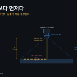
The Lens Comes Before the AI — Optical Setup Design for PCB Inspection
When an AOI starts missing solder bridges on one lot, most engineers suspect the model first. More often the real cause is the lens spec sheet and the lighting angle.
-
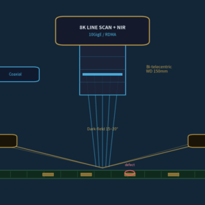
In the Age of 8K Line-Scan Cameras, the Lens Still Sets the Ceiling on Inspection Resolution
Upgrading to an 8K line-scan camera and still leaking micro-defects? Effective resolution is set by lens MTF and lighting, not sensor pixel count.
-
The Defect Zone You Miss When You Switch to 3D Inspection
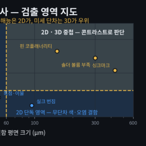
A 3D profiler's planar (xy) resolution is coarser than 2D line-scan. See how to route defects between 2D and 3D by measured contrast, not size, with WD and optical-setup specs.